Input/Output Coupling Structure for Dielectric Waveguide

Active Publication Date: 2012-08-16
MURATA MFG CO LTD
View PDF3 Cites 17 Cited by
  • Summary
  • Abstract
  • Description
  • Claims
  • Application Information

AI Technical Summary

Benefits of technology

[0021]The dielectric waveguide input/output coupling structure of the present invention can exhib

Problems solved by technology

However, the dielectric waveguide, and a strip line used in the printed circuit board,

Method used


Image

  • Input/Output Coupling Structure for Dielectric Waveguide
  • Input/Output Coupling Structure for Dielectric Waveguide
  • Input/Output Coupling Structure for Dielectric Waveguide

Examples


Embodiment Construction

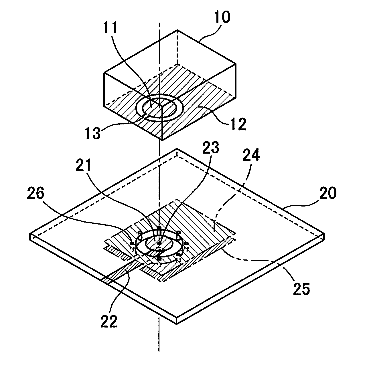
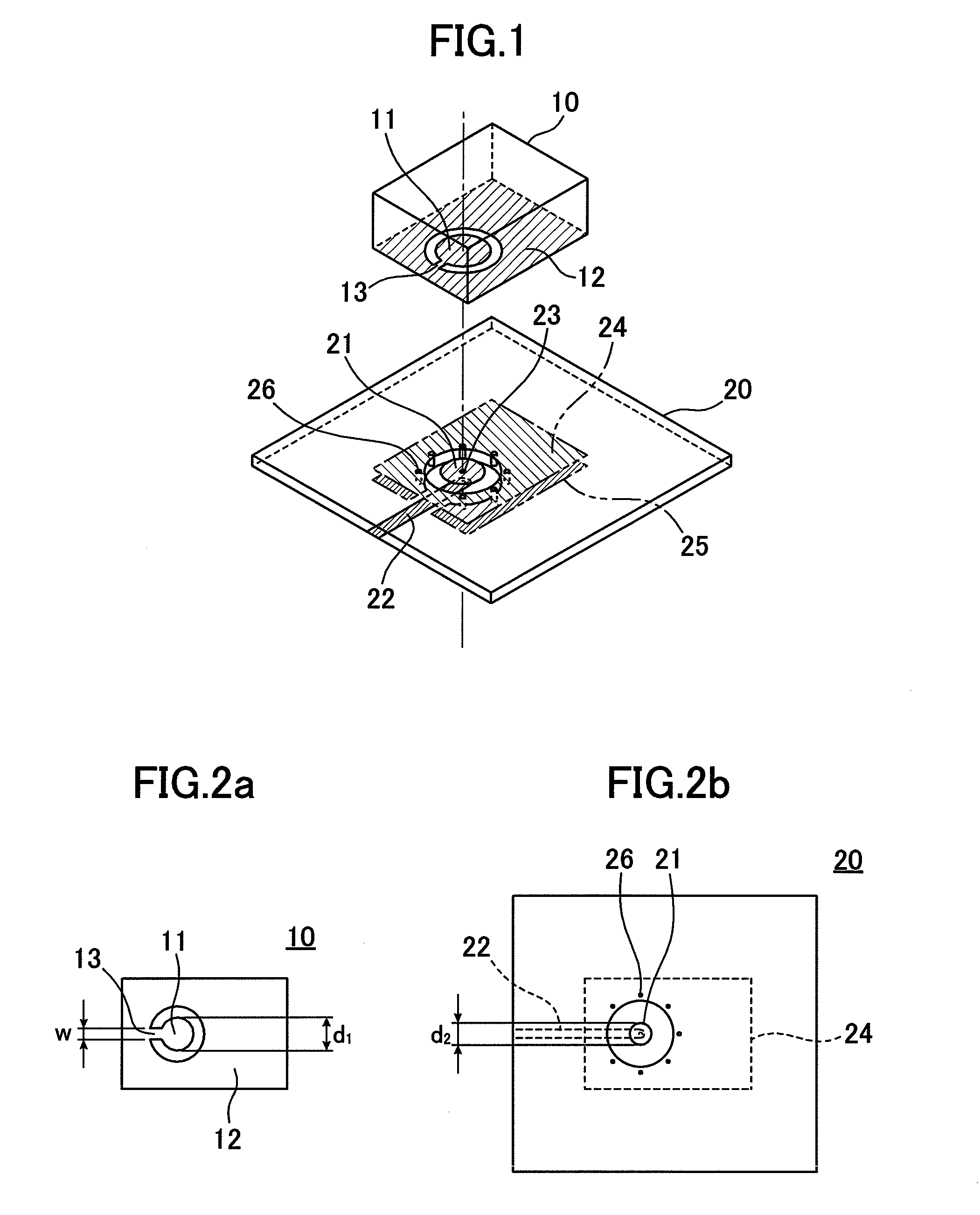
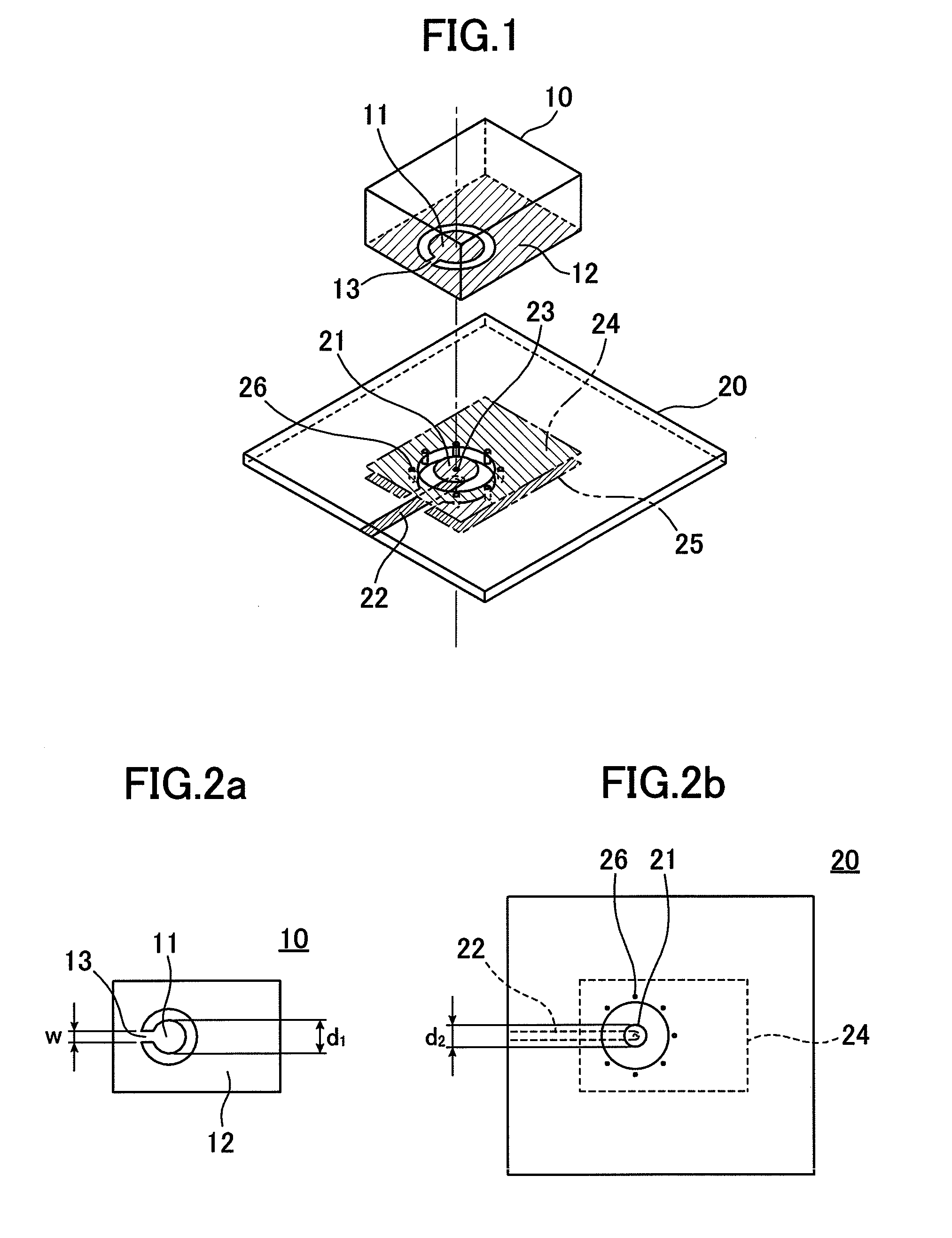
[0028]FIG. 1 is an exploded perspective view illustrating a dielectric waveguide input / output coupling structure according to one embodiment of the present invention.

[0029]As illustrated in FIG. 1, a dielectric waveguide 10 comprises a dielectric block composed of a rectangular parallelepiped-shaped dielectric, and a conductor film 12 covering an exterior of the dielectric block, wherein the dielectric waveguide 10 has a bottom surface having a generally circular input / output electrode 11 made of a conductor and surrounded by an exposed dielectric portion (i.e., an exposed portion of the dielectric) of the dielectric waveguide 10. The input / output electrode 11 and the conductor film 12 are coupled together via a short (short-circuiting) stub 13 made of a conductor and formed to cross through the exposed dielectric portion.

[0030]On the other hand, a printed circuit board 20 has a front surface having: a generally-circular island-shaped electrode 21 made of a conductor; and a front su...


PUM


Abstract

Dielectric waveguide comprising a circular input/output electrode on its bottom surface and surrounded by an exposed dielectric portion thereof around which a conductor film is disposed. A short stub crosses through the exposed dielectric portion to couple the electrode and film together. The printed circuit board has a front surface formed with a generally-circular island-shaped electrode surrounded by a front surface-side ground pattern in a spaced-apart relation thereto, and a back surface formed with a strip line surrounded by a back surface-side ground pattern in spaced-apart relation thereto. An approximate center of the island-shaped electrode and one end of the strip line are coupled together, and the front surface-side ground pattern and the back surface-side pattern are coupled together. The input/output electrode of the dielectric waveguide and the island-shaped electrode of the printed circuit board are coupled together.

Description

[0001]TECHNICAL FIELD[0002]The present invention relates to an input / output coupling structure between a dielectric waveguide and a printed circuit board on which the dielectric waveguide is to be mounted, and, more particularly, to a bandwidth widening technique for the input / output coupling structure.BACKGROUND ART[0003]In late years, mobile communications devices have become widespread, and frequency bands up to about 2 GHz band have come to be used in mobile communications. In a base station for communications in such frequency bands, a dielectric waveguide filter has been used which comprises a combination of a plurality of resonators each composed of a dielectric waveguide.[0004]The dielectric waveguide filter is capable of facilitating downsizing and weight reduction based on a wavelength shortening effect of dielectric, and thereby can be directly mounted on a printed circuit board.[0005]However, the dielectric waveguide, and a strip line used in the printed circuit board, a...

Claims


Application Information

Patent Timeline
IPC IPC(8): H01P5/107
CPCH01P5/107H01P5/087H01P1/2088H01P3/16H01P3/08
Inventor KOJIMA, HIROSHIYABE, TAKAYUKIITO, KAZUHIRO
Owner MURATA MFG CO LTD
Why Eureka
Try Eureka