Light-Emitting Device and Electronic Device Using Light-Emitting Device

a technology of light-emitting devices and electronic devices, applied in the direction of solid-state devices, electric lighting sources, electric lighting sources, etc., can solve the problems of light-emitting elements being damaged and separated, and achieve the effect of high reliability and preventing damag

Active Publication Date: 2012-08-30
SEMICON ENERGY LAB CO LTD
View PDF6 Cites 209 Cited by
  • Summary
  • Abstract
  • Description
  • Claims
  • Application Information

AI Technical Summary

Benefits of technology

[0024]A highly reliable light-emitting device is provided in which a light-emitting element is prevented from being damaged when external physical force is applied to the light-emitting device provided with the light-emitting element including a light-emitting layer provided between a pair of electrodes.

Problems solved by technology

In addition, in the case of a light-emitting device using a flexible substrate, there is a possibility that separation may occur at the interface between the light-emitting layer and the electrode, and the light-emitting element may be damaged when physical force such as bending or curving is externally applied.

Method used


Image

  • Light-Emitting Device and Electronic Device Using Light-Emitting Device
  • Light-Emitting Device and Electronic Device Using Light-Emitting Device
  • Light-Emitting Device and Electronic Device Using Light-Emitting Device

Examples


embodiment 1

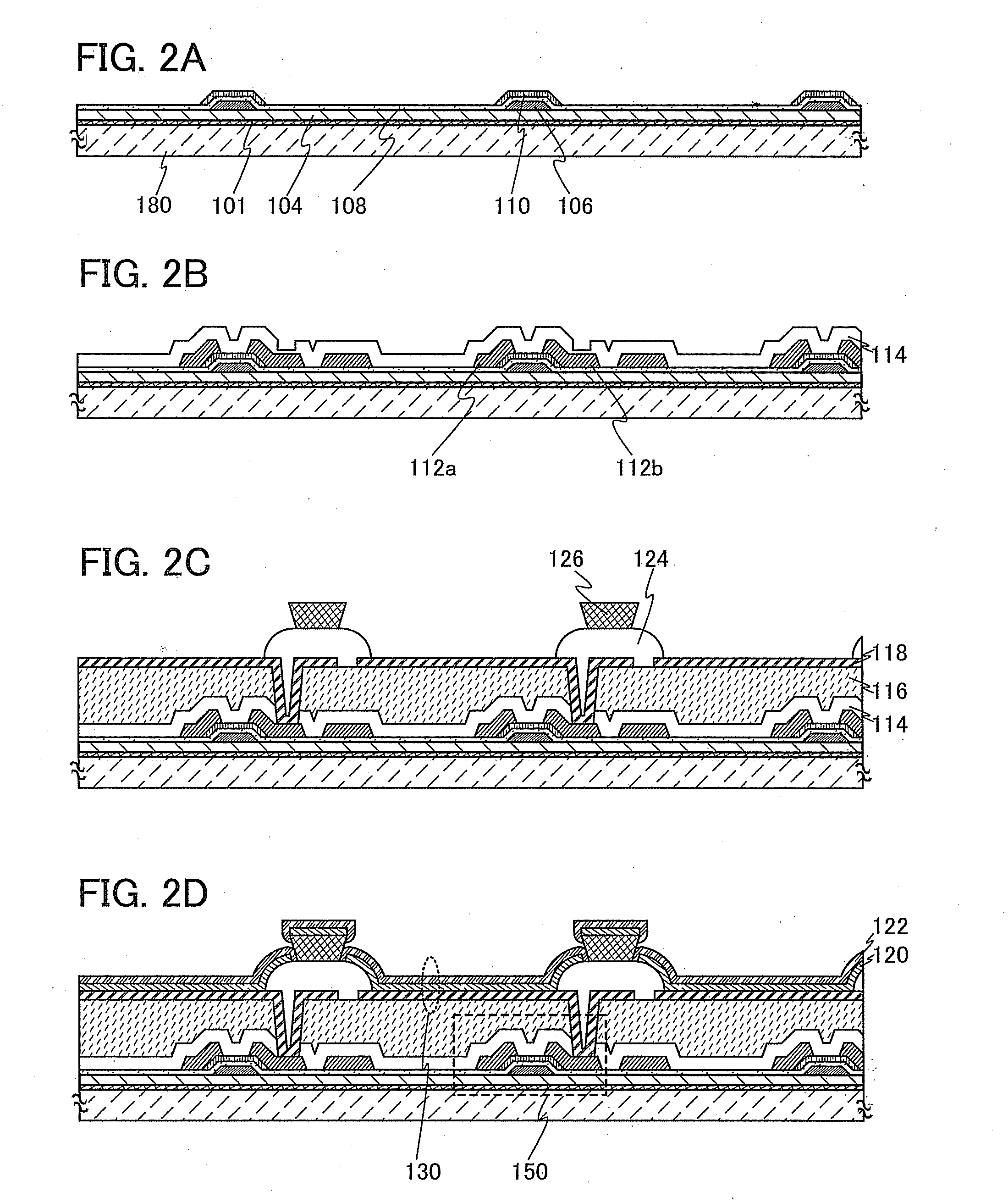
[0039]In this embodiment, according to one embodiment of a light-emitting device of the present invention, a structure of the light-emitting device is described with reference to FIGS. 1A and 1B, and then a method for manufacturing the light-emitting device is described with reference to FIGS. 2A to 2D, FIGS. 3A to 3C, FIGS. 4A and 4B, and FIGS. 5A and 5B.

Structure of Light-Emitting Device

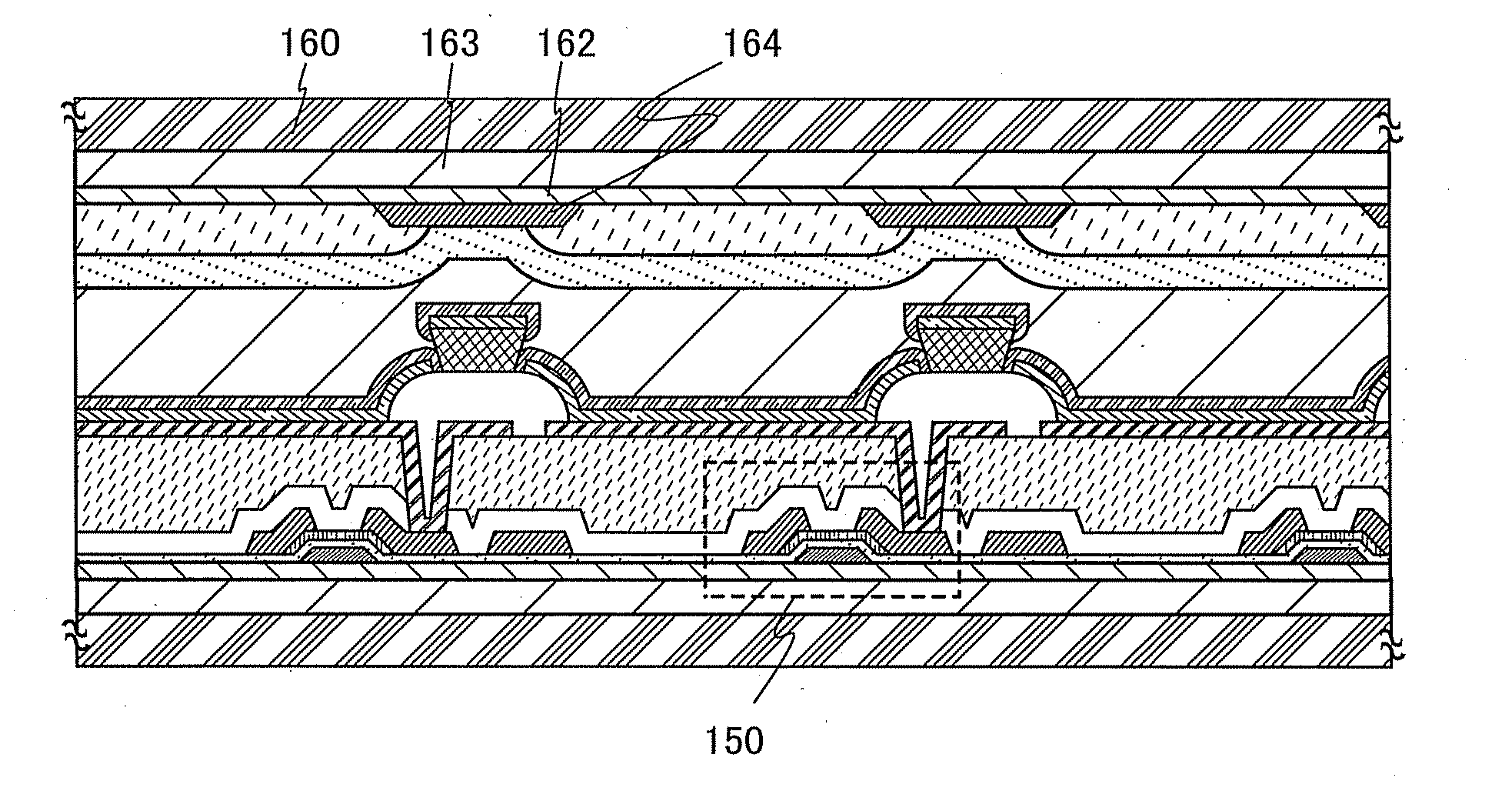
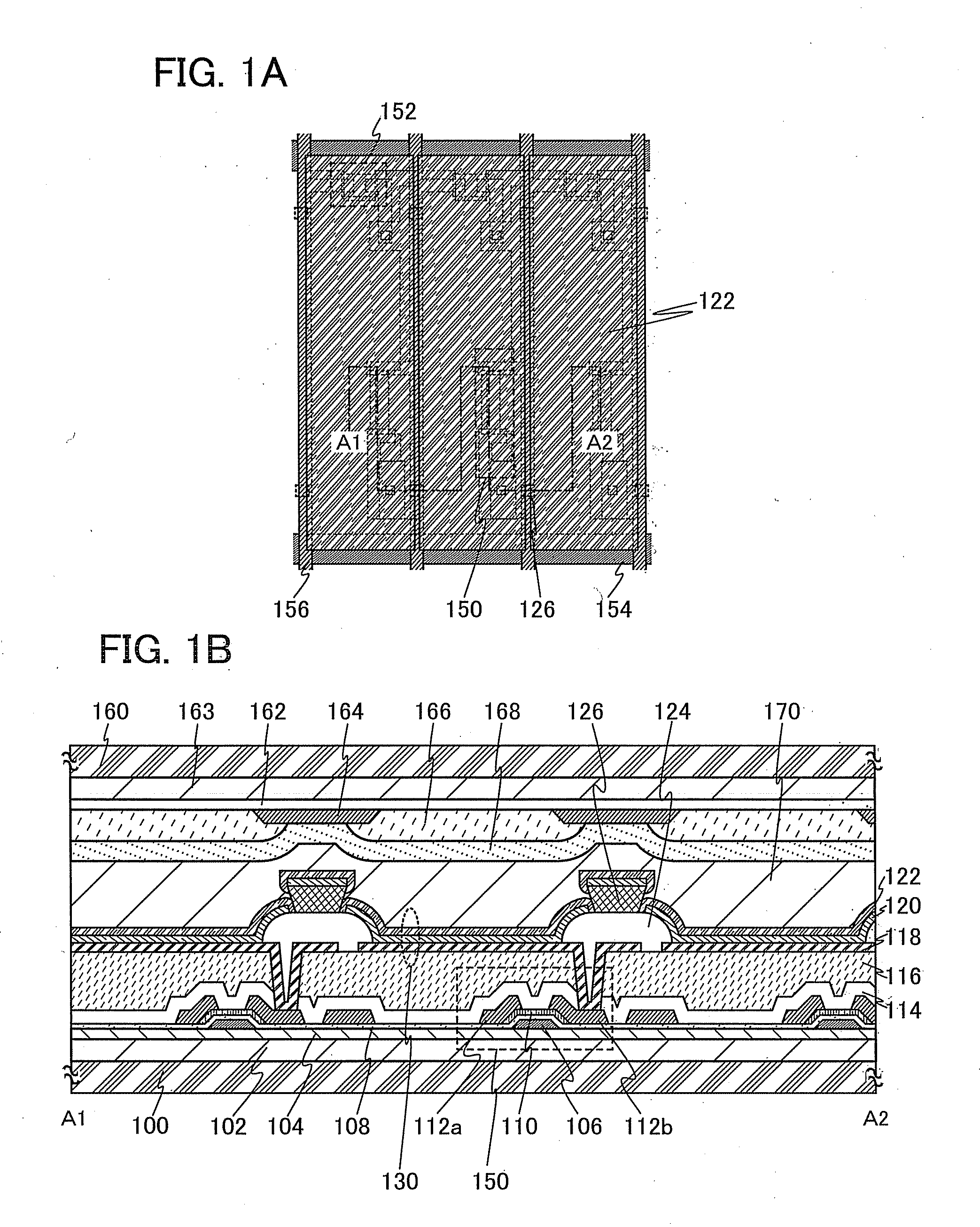
[0040]FIG. 1A is a top view of a first substrate 100 seen from a second electrode layer 122 side, which illustrates a part of a pixel of the light-emitting device. FIG. 1B is a cross-sectional view taken along broken line A1-A2 in FIG. 1A. In the top view of FIG. 1A, some components (e.g., a partition wall 124, and the like) of the present invention are omitted in order to avoid complex views.

[0041]In the light-emitting device shown in FIG. 1A, a plurality of source wirings 156 is provided parallel to (extending in the vertical direction in the drawing) and apart from each other, and a plurality of...

embodiment 2

[0130]A structure body used for a light-emitting device of the present invention, which has a different structure from the structure body 126 described in Embodiment 1, will be described with reference to FIGS. 6A to 6D.

[0131]Note that the same reference numerals are used for the same parts as those of the light-emitting device in Embodiment 1, and description of the parts with the same reference numerals will be omitted here.

[0132]The light-emitting device shown in FIG. 6A has a structure body 206 including a first structure body 202 and a second structure body 204 over the partition wall 124.

[0133]As a method for forming the structure body 206, a film formed of an organic insulating material is formed; then, a film formed of an inorganic insulating material is formed thereover. After that patterning is performed on a desired region, the film formed of the inorganic insulating material is processed, and then the film formed of the organic insulating material is processed using the ...

embodiment 3

[0153]In this embodiment, description is made on the arrangement of pixels of light-emitting devices in which the structure body 126 described in Embodiment 1 and the structure bodies 206, 208, 210, and 214 described in Embodiment 2 are used with reference to FIGS. 7A to 7D.

[0154]FIGS. 7A to 7D are top views of part of pixels of the light-emitting device. In this embodiment, the position of the structure body in each pixel is described; thus, some components (for example, the transistor 150, the light-emitting element 130, and the like) of the present invention are omitted in order to avoid complex views each of the light-emitting devices shown in FIGS. 7A to 7D, a plurality of source wirings 156 is provided parallel to (extending in the vertical direction in the drawing) and apart from each other, and a plurality of gate wirings 154 is provided parallel to (extending in the horizontal direction in the drawing) and apart from each other. A substantially rectangular region is surroun...


PUM


Abstract

Provided is a highly reliable light-emitting device in which a light-emitting element is prevented from being damaged when external physical force is applied. The light-emitting device includes a light-emitting element formed over a first substrate, including a first electrode layer, a light-emitting layer, and a second electrode layer; a structure body formed over the first substrate; a second substrate provided to face the first substrate; and a bonding layer provided between the first substrate and the second substrate. The light-emitting layer is separated by the structure body. By strengthening adhesion between the structure body and the bonding layer, or between the structure body and the second electrode, the highly reliable light-emitting device in which damage of the light-emitting element is prevented can be provided.

Description

TECHNICAL FIELD[0001]One embodiment of the present invention relates to a light-emitting device utilizing electroluminescence. Further, an embodiment of the present invention relates to an electronic device using the light-emitting device.BACKGROUND ART[0002]In recent years, research and development have been extensively conducted on light-emitting elements using electroluminescence (EL). In a basic structure of such a light-emitting element, a layer containing a light-emitting substance is provided between a pair of electrodes. By applying voltage to this element, light emission can be obtained from the light-emitting substance.[0003]Since the above light-emitting element is a self-luminous type, a light-emitting device using this light-emitting element has advantages such as high visibility, no necessity of a backlight, low power consumption, and the like. Further, such a light-emitting element also has advantages in that the element can be formed to be thin and lightweight and th...

Claims


Application Information

Patent Timeline
Patent Type & Authority Applications(United States)
IPC IPC(8): H01L33/08H05B44/00
CPCH01L51/525H01L27/3246H10K59/122H10K50/8428H10K50/125H10K50/805H10K50/11H10K2102/311
Inventor HATANO, KAORUSEO, SATOSHICHIDA, AKIHIROOIKAWA, YOSHIAKI
Owner SEMICON ENERGY LAB CO LTD
Why Eureka
Try Eureka