Method of manufacturing film for semiconductor device

Inactive Publication Date: 2012-09-13
NITTO DENKO CORP
View PDF3 Cites 3 Cited by
  • Summary
  • Abstract
  • Description
  • Claims
  • Application Information

AI Technical Summary

Benefits of technology

[0010]The present inventors investigated a method of manufacturing a film for a semiconductor device, and a film for a semiconductor device to solve the above-described conventional problems. As a result, they found that a method of manufacturing a film for a semiconductor device in which the die bond film is located at the center of the dicing film and the film for a semiconductor device can be provided by adopting the following configuration, and completed the present invention.

Problems solved by technology

There is a case where a die bond film cannot be punched out accurately so that the die bond film comes to the center in a conventional manufacturing method, and there has been a problem that such a case causes a decrease of manufacturing yield of the dicing film with a die bond film.

Method used


Image

  • Method of manufacturing film for semiconductor device
  • Method of manufacturing film for semiconductor device
  • Method of manufacturing film for semiconductor device

Examples


manufacturing example 1

[0111]In methylethylketone were dissolved 12 parts of an epoxy resin (Epicoat 1004 manufactured by JER), 13 parts of a phenol resin (Milex XLC-4L manufactured by Mitsui Chemicals, Inc.), 100 parts of an acrylic ester polymer having ethylacrylate-methylmethacrylate as a main component (SG-708-6 manufactured by Nagase ChemteX Corporation), and 30 parts of spherical silica (SO-25R manufactured by Admatechs Co., Ltd.) as a filler to obtain an adhesive composition solution having a concentration of 23.6% by weight.

[0112]This adhesive composition solution was applied onto a release-treated film (a release liner) made from polyethylene terephthalate and having a thickness of 50 μm which had been subjected to a silicone releasing treatment, and the resultant was dried at 130° C. for 2 minutes to produced a die bond film A having a thickness of 20 μm.

manufacturing example 2

[0113]In methylethylketone were dissolved 48 parts of an epoxy resin (Epicoat 1004 manufactured by JER), 51 parts of a phenol resin (Milex XLC-4L manufactured by Mitsui Chemicals, Inc.), 100 parts of an acrylic ester polymer having ethylacrylate-methylmethacrylate as a main component (SG-708-6 manufactured by Nagase ChemteX Corporation), and 74 parts of spherical silica (SO-25R manufactured by Admatechs Co., Ltd.) as a filler to obtain an adhesive composition solution having a concentration of 23.6% by weight.

[0114]This adhesive composition solution was applied onto a release-treated film (a release liner) made from polyethylene terephthalate and having a thickness of 50 μm which had been subjected to a silicone releasing treatment, and the resultant was dried at 130° C. for 2 minutes to produced a die bond film B having a thickness of 20 μm.

manufacturing example 3

[0115]In methylethyl ketone were dissolved 193 parts of an epoxy resin (Epicoat 1004 manufactured by JER), 207 parts of a phenol resin (Milex XLC-4L manufactured by Mitsui Chemicals, Inc.), 100 parts of an acrylic ester polymer having ethylacrylate-methylmethacrylate as a main component (SG-708-6 manufactured by Nagase ChemteX Corporation), and 195 parts of spherical silica (SO-25R manufactured by Admatechs Co., Ltd.) as a filler to obtain an adhesive composition solution having a concentration of 23.6% by weight.

[0116]This adhesive composition solution was applied onto a release-treated film (a release liner) made from polyethylene terephthalate and having a thickness of 50 μm which had been subjected to a silicone releasing treatment, and the resultant was dried at 130° C. for 2 minutes to produced a die bond film C having a thickness of 20 μm.


PUM


Abstract

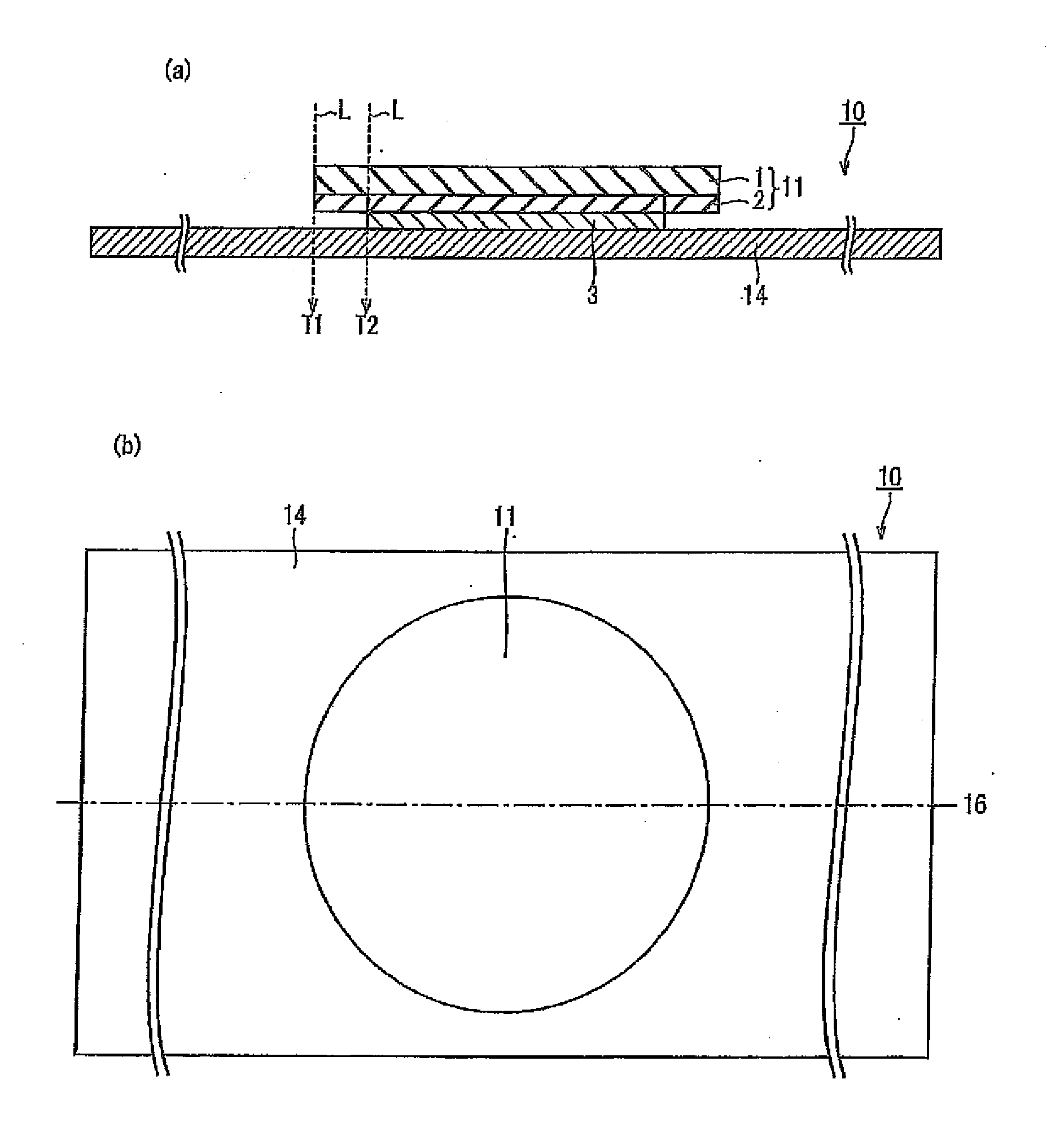
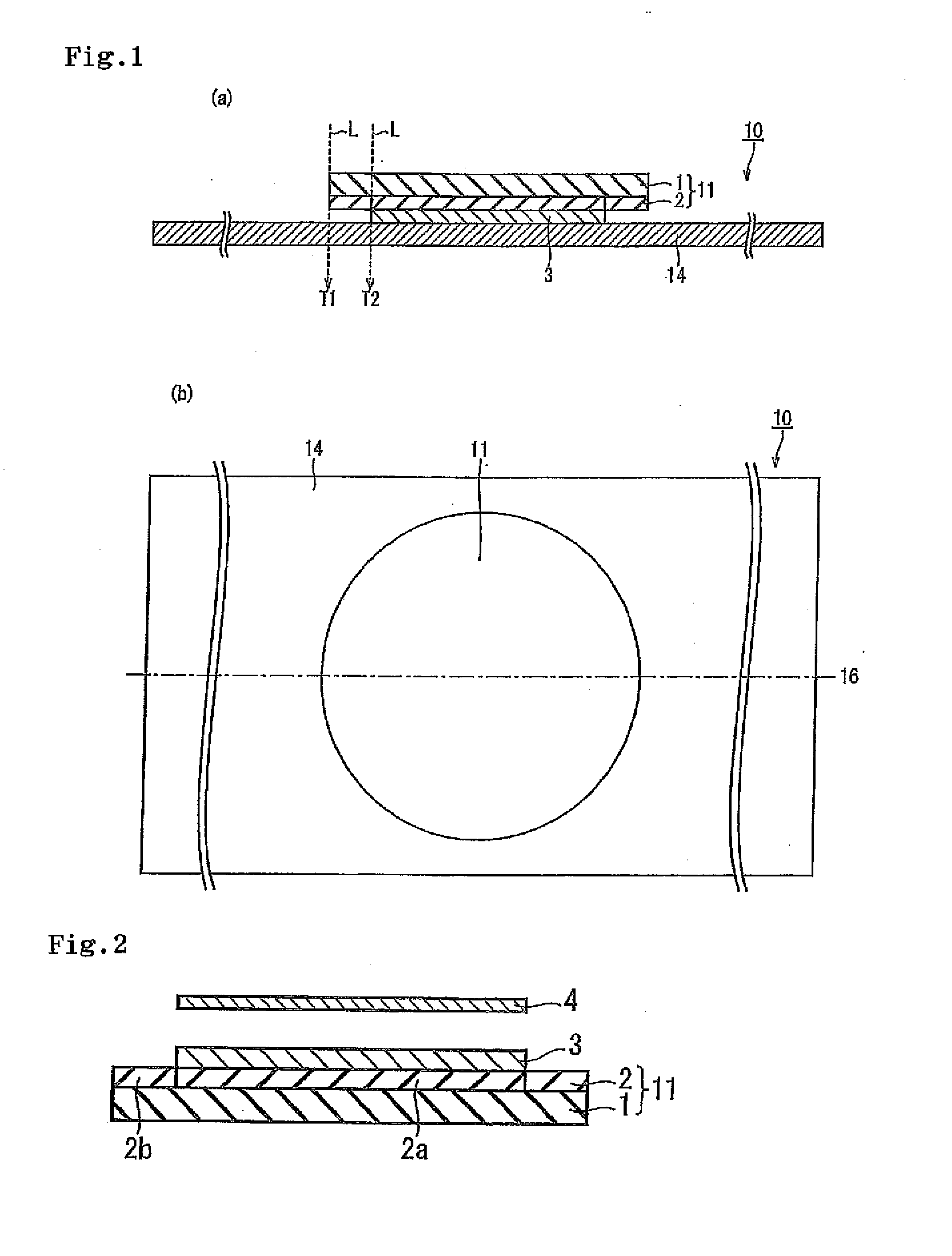
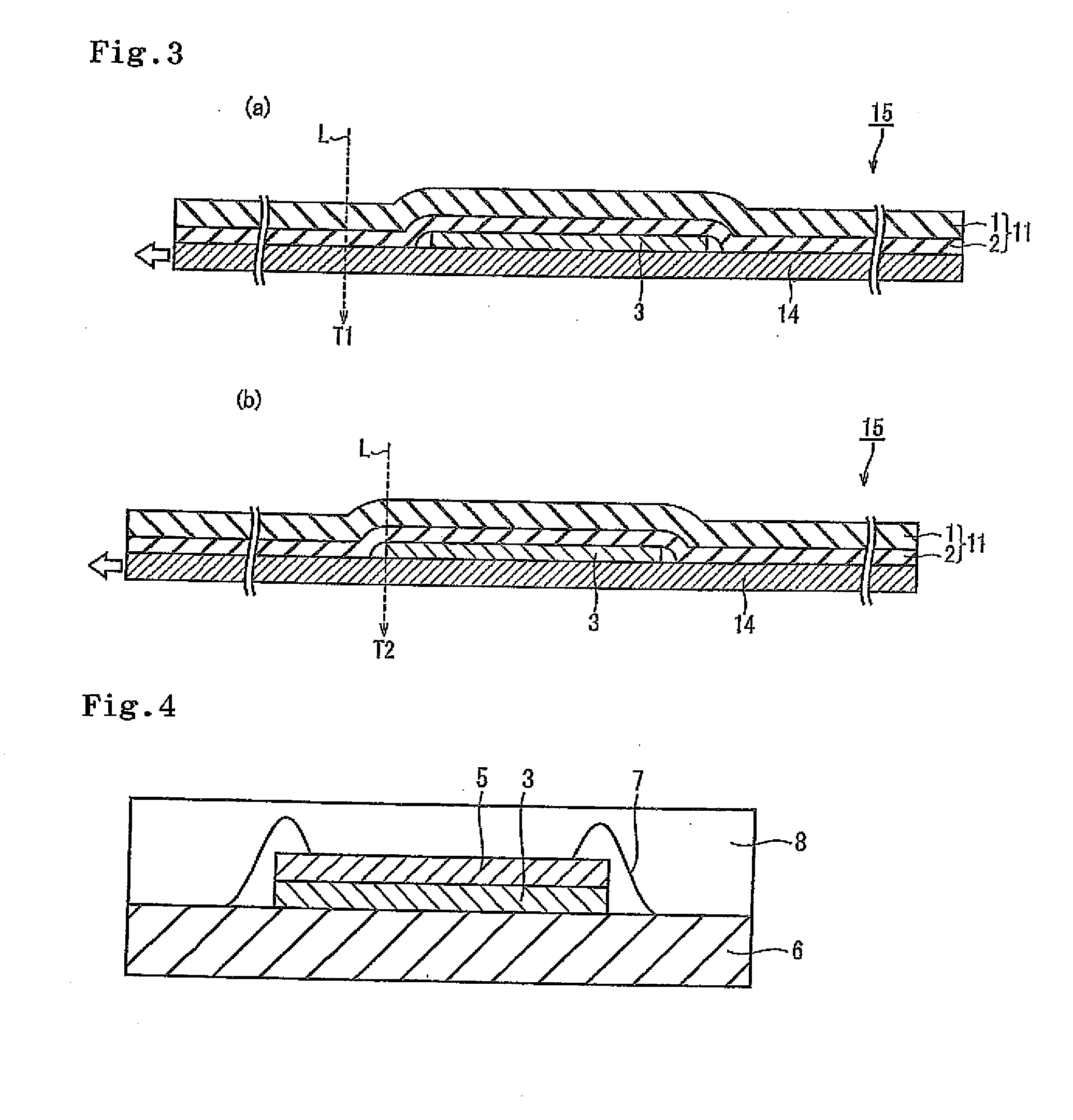
The present invention aims to provides a method of manufacturing a film for a semiconductor device in which a dicing film, a die bond film, and a protecting film are laminated in this order, including the steps of: irradiating the die bond film with a light ray having a wavelength of 400 to 800 nm to detect the position of the die bond film based on the obtained light transmittance and punching the dicing film out based on the detected position of the die bond film, and in which T2 / T1 is 0.04 or more, wherein T1 is the light transmittance of the portion where the dicing film and the protecting film are laminated and T2 is the light transmittance of the portion where the dicing film, the die bond film, and the protecting film are laminated.

Description

BACKGROUND OF THE INVENTION[0001]1. Field of the Invention[0002]The present invention relates to a method of manufacturing a film for a semiconductor device.[0003]2. Description of the Related Art[0004]Conventionally, a semiconductor wafer is manufactured to have a large area in advance, diced into chips (separation by cutting), and transferred to an expanding step. A dicing film is used to fix the semiconductor wafer when dicing.[0005]The semiconductor wafer that is fixed to the dicing film is diced into chips, and expanded uniformly in the surface direction on an expansion ring to separate each chip, and then the chips are picked up.[0006]A dicing film has been conventionally proposed in Japanese Patent Application Laid-Open No. 60-57642, that adheres and holds a semiconductor wafer in a dicing step and also yields a die bond film for fixing a chip that is necessary in a mounting step.[0007]The dicing film with a die bond film as described above can be obtained by, for example, (1...

Claims


Application Information

Patent Timeline
IPC IPC(8): H01L21/66
CPCH01L21/56H01L2924/01047H01L21/6836H01L21/78H01L24/83H01L24/85H01L2221/68327H01L2221/68377H01L2221/68381H01L24/29H01L24/32H01L24/48H01L24/92H01L2224/2919H01L2224/45124H01L2224/45144H01L2224/45147H01L2224/73265H01L2224/83191H01L2224/83862H01L2224/83906H01L2224/85205H01L2224/9205H01L2224/92247H01L2224/32225H01L2224/48227H01L2224/32245H01L2924/00013H01L2224/48247H01L2924/01012H01L2924/01013H01L2924/01014H01L2924/01028H01L2924/01029H01L2924/15747C09J2203/326H01L24/45H01L2924/3025H01L2224/48091H01L2924/01015H01L21/67132H01L2924/00014H01L2924/00H01L2224/13099H01L2224/13599H01L2224/05599H01L2224/05099H01L2224/29099H01L2224/29599H01L2924/3512H01L2924/00012H01L24/73H01L2924/15788H01L2924/181H01L21/30
Inventor INOUE, KOICHIMORITA, MIKISHISHIDO, YUICHIRO
Owner NITTO DENKO CORP
Why Eureka
Try Eureka