Semiconductor laser device and manufacturing method therefor

Inactive Publication Date: 2010-04-15
SHARP KK
View PDF11 Cites 9 Cited by
  • Summary
  • Abstract
  • Description
  • Claims
  • Application Information

AI Technical Summary

Benefits of technology

[0062]According to the semiconductor laser device of the present invention, since the mounting of the nitride semiconductor laser element is performed so that the width of the conductive adhesive becomes smaller than that of the nitride semiconductor laser element, crawl-up of the conductive adhesive onto the side faces of the nitride semiconductor laser element can be prevented.
[0063]Accordingly, short-circuits due to the sticking of the conductive adhesive on the side faces of the nitride semiconductor laser element can be prevented, so that the issue of decreases in manufacturing yield can be solved.
[0064]Also, since the sticking of the conductive adhesive onto the side faces of the nitride semiconductor laser element can be eliminated, device reliability can be enhanced.
[0065]According to the semiconductor laser device manufacturing method of the present invention, the width to which the conductive adhesive is formed in the formation step is so predetermined that the width of the conductive adhesive after the mounting step becomes smaller than the width of the nitride semiconductor laser element. Therefore, it becomes possible to prevent the conductive adhesive from crawling up onto the side faces of the nitride semiconductor laser element even though the nitride semiconductor laser element is placed on the conductive adhesive.
[0066]Accordingly, short-circuits due to the sticking of the conductive adhesive on the side faces of the nitride semiconductor laser element can be prevented, so that the issue of decreases in manufacturing yield can be solved.
[0067]Also, since the sticking of the conductive adhesive onto the side faces of the nitride semiconductor laser element can be eliminated, device reliability can be enhanced.

Problems solved by technology

As a result, in the nitride semiconductor laser element, there may arise a failure that p-type nitride semiconductor and n-type nitride semiconductor are short-circuited to each other via solder, leading to decreases in yield as a problem.

Method used


Image

  • Semiconductor laser device and manufacturing method therefor
  • Semiconductor laser device and manufacturing method therefor
  • Semiconductor laser device and manufacturing method therefor

Examples


first embodiment

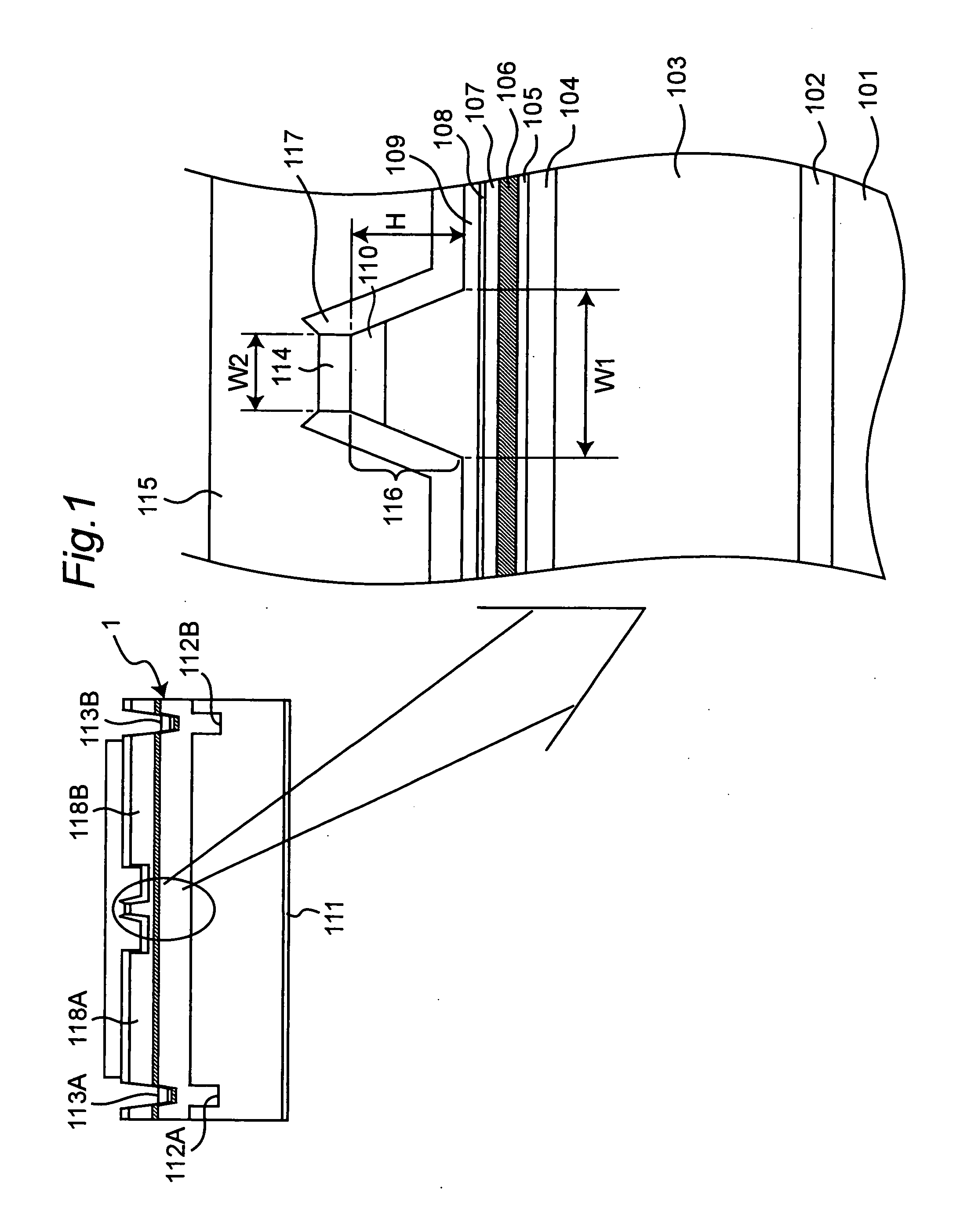
[0090]FIG. 1 is a schematic sectional view of a nitride semiconductor laser element 1 according to a first embodiment of the invention.

[0091]The nitride semiconductor laser embodiment 1 includes an n-type (hereinafter, n conductive type will be referred to as “n-” and p conductive type as “p-”) GaN substrate 101. The nitride semiconductor laser element further includes, as layers formed on the n-GaN substrate 101 on one another, a 0.5 μm thick n-GaN layer 102, a 2 μm thick n-Al0.05Ga0.95N lower clad layer 103, a 0.1 μm thick n-GaN guide layer 104, a 20 nm thick GaN lower adjoining layer 105, an active layer 106, a 50 nm thick GaN upper adjoining layer 107, a 20 nm thick p-Al0.2Ga0.8N carrier barrier layer 108, a 0.6 μm thick p-Al0.1Ga0.9N upper clad layer 109, and a 0.1 μm p-GaN contact layer 110. Then, nitride semiconductors are exposed from a side face of the nitride semiconductor laser element 1. Further, crack preventing grooves 113A, 113B are formed on an upper surface (a surfa...

second embodiment

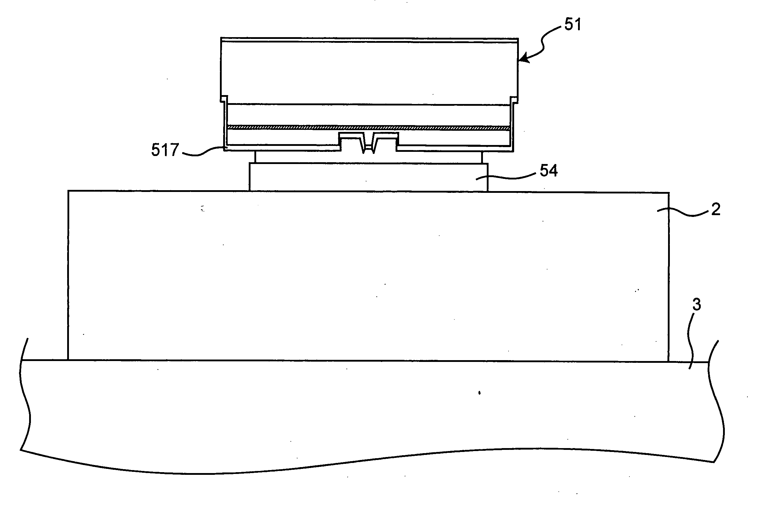
[0147]FIG. 9 is a schematic sectional view of a nitride semiconductor laser element 31 according to a second embodiment of the invention.

[0148]This nitride semiconductor laser element 31 includes a dielectric film 317, and the dielectric film 317 covers part of side faces of the nitride semiconductor laser element 31 as well as crack preventing grooves 313A, 313B. It is noted that the dielectric film 317 is an example of the dielectric.

[0149]In fabrication of the nitride semiconductor laser element 31, first as in the first embodiment, on an n-GaN substrate are layer-stacked an n-GaN layer, an n-Al0.1Ga0.9N lower clad layer, an n-GaN guide layer, a GaN lower adjoining layer, an active layer, a GaN upper adjoining layer, a p-Al0.2Ga0.8N carrier barrier layer, a p-Al0.1Ga0.9N upper clad layer, and a p-GaN contact layer layer-stacked one after another, and thereafter ridge portions and terrace portions are formed.

[0150]Next, 5 μm deep grooves are formed at chip dividing portion surroun...

third embodiment

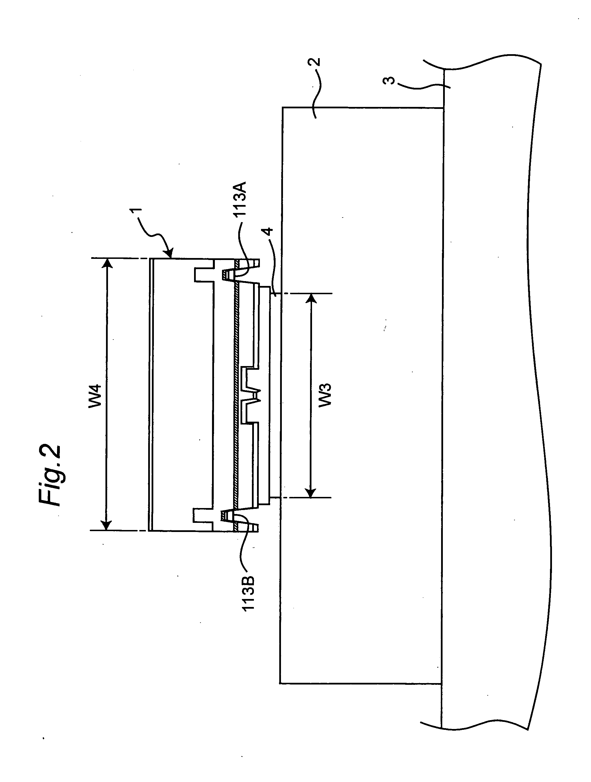
[0156]FIG. 11 is a schematic front view of a nitride semiconductor laser device according to a third embodiment of the invention. In FIG. 11, the same component members as those of the first embodiment shown in FIG. 2 are designated by the same reference numerals as those of FIG. 2 and their description is omitted.

[0157]This nitride semiconductor laser device includes a nitride semiconductor laser element 41 mounted on the surface of the submount 2 with solder 44. It is noted that the solder 44 is an example of the conductive adhesive and differs from the solder 4 of the first embodiment only in its shape.

[0158]The nitride semiconductor laser element 41 is not a ridge stripe type one, but an internal constriction structure type one. More specifically, the nitride semiconductor laser element 41 has an n-GaN substrate 401, a current constriction layer 402, an active layer 403, a p-contact electrode 404, a p-side electrode 405, and an n-side electrode 406. Then, in the nitride semicond...


PUM


Abstract

Provides a semiconductor laser device, as well as a manufacturing method therefor, capable of solving a problem of yield decreases in a structure for mounting a nitride semiconductor laser element onto a mount member. The nitride semiconductor laser device has a submount 2, and a nitride semiconductor laser element 1 which is mounted on a surface of the submount 2 with a solder 4 so that a nitride semiconductor is exposed from a side face thereof. The solder 4 is positioned between the submount 2 and the nitride semiconductor laser element 1 and has a width W3 smaller than a lateral width W4 of the nitride semiconductor laser element 1.

Description

TECHNICAL FIELD[0001]The present invention relates to a semiconductor laser device, as well as its manufacturing method, which includes a nitride semiconductor laser element formed from III-V group nitride semiconductor.BACKGROUND ART[0002]The nitride semiconductor laser element has been receiving attention as a short-wavelength light source for performing read and write of information on high-density optical recording mediums. Further, the nitride semiconductor laser element, being capable of wavelength conversion of emitted light to a visible region, is expected also as a light source for visible light of illumination, backlight and the like. Then, with a view to expanding applications of the nitride semiconductor laser element, techniques for stabilizing its operations or enhancing its output power have been developed and discussed. When the nitride semiconductor laser element is enhanced to higher power, heat sink measures for efficiently dissipating heat generation of the nitri...

Claims


Application Information

Patent Timeline
IPC IPC(8): H01S5/00H01L33/00
CPCB82Y20/00H01S5/0021H01S5/0224H01S5/02272H01S5/028H01S5/34333H01S5/2009H01S5/22H01S5/2201H01S5/2214H01S5/3063H01S5/0425H01L24/32H01S5/04254H01S5/0234H01S5/0237
Inventor TAKAHIRA, YOSHIYUKI
Owner SHARP KK
Why Eureka
Try Eureka