Process for treating a semiconductor-on-insulator structure
Active Publication Date: 2012-09-13
S O I TEC SILICON ON INSULATOR THECHNOLOGIES
View PDF19 Cites 6 Cited by
Summary
Abstract
Description
Claims
Application Information
AI Technical Summary
This helps you quickly interpret patents by identifying the three key elements:
Problems solved by technology
Method used
Benefits of technology
Benefits of technology
[0018]In accordance with the invention, a process is provided for treating a semiconductor-on-insulator structure comprising in succession a support substrate, a layer of the oxide or oxynitride of a semiconductor material, and a thin semiconductor layer of the semiconductor material. In one embodiment, the process comprises masking the surface of the thin layer to provide exposed regions and mas
Problems solved by technology
The use of such a mask may have certain drawbacks, however, including the appearance, in the thin semiconductor layer, of trenches at the mask edge.
These topographical defects, the depth of which may reach the thickness of the semiconductor layer, are detrimental to the fabrication of components on the thin semiconductor layer.
In particular, the mask-edge defects amplify the surface topography variation.
This variation makes subsequent circuit fabrication steps difficult to carry out and may lead to dewetting of the semiconductor, i.e., to a loss of cohesion in the thin semiconductor layer, wh
Method used
Image
Click on the blue label to locate the original text in one second.
Reading with bidirectional positioning of images and text.
Examples
Example
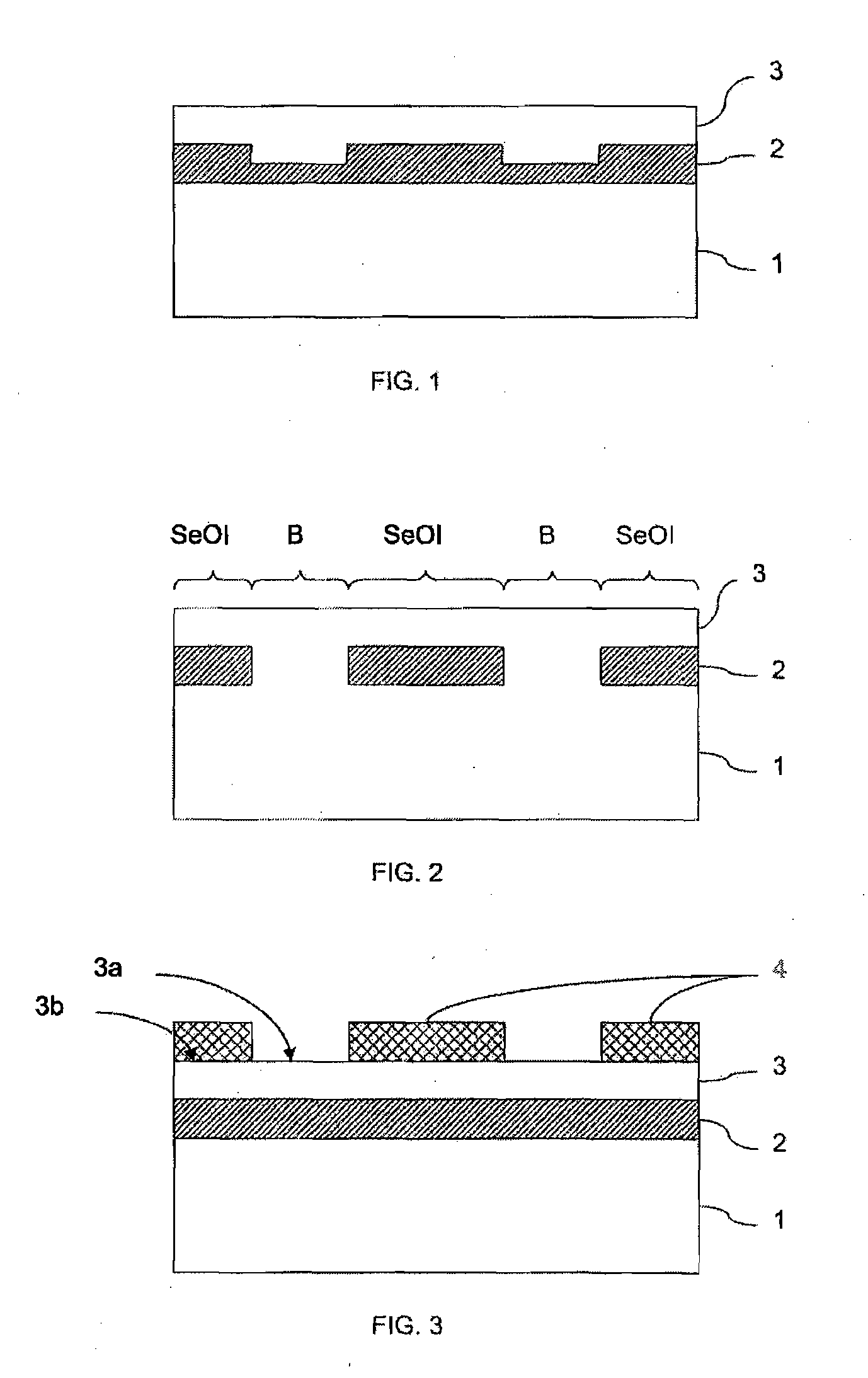
[0075]Thus, according to a first embodiment, the mask is produced by local deposition of a nitride or oxide on the surface of the thin layer 3.
Example
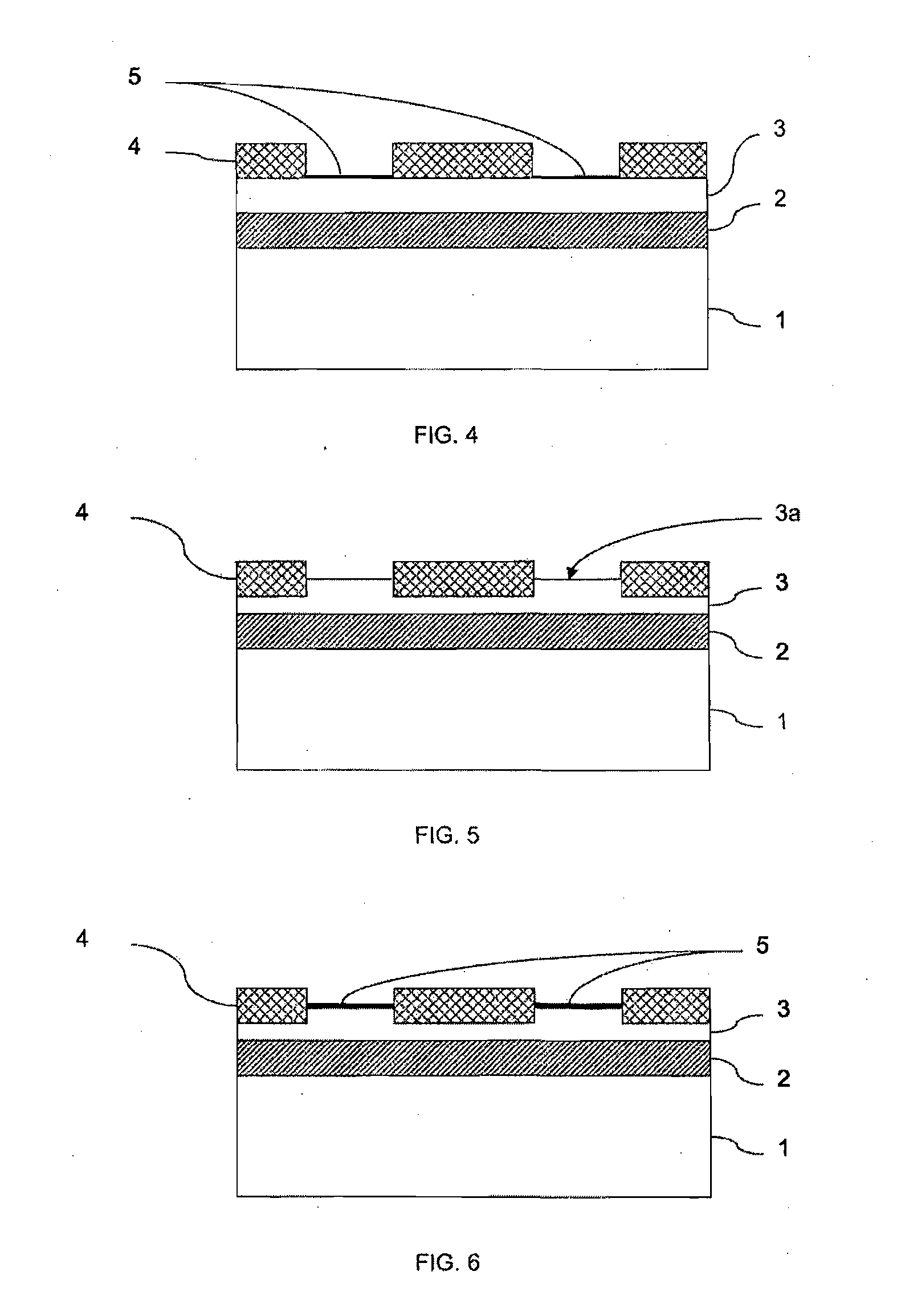
[0076]According to a second embodiment, illustrated in FIG. 5, the mask is formed by thermal oxidation of zones of the thin layer 3b, the zones 3a intended to form the exposed zones being protected from such oxidation.
[0077]Relative to the preceding embodiment, the formation of such a mask involves a small thickness of the thin layer 3 being consumed, leading to the mask being partially “buried” in the thin layer 3.
Example
[0078]According to a third embodiment (not illustrated here), the mask consists of regions of the thin layer 3 which are thicker than the regions through which the oxygen, and if required nitrogen, atoms must diffuse from the buried oxide or oxynitride layer.
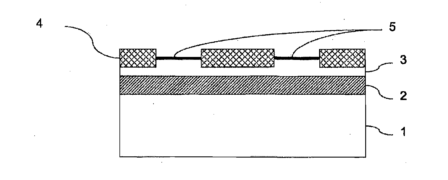
[0079]Treatment of the Exposed Regions
[0080]With reference to FIG. 4, or if appropriate to FIG. 6, after the mask 4 has been formed, a treatment is applied to the exposed regions 3a of the thin layer 3, the treatment aiming to form, on the surface of such regions 3a, a thin layer 5 of the nitride or oxynitride of the semiconductor of the layer 3.
[0081]According to a first embodiment, the treatment is carried out before the dissolution heat treatment is implemented.
[0082]The treatment may comprise applying a nitrogen plasma.
[0083]By way of example, an N2 RIE (reactive ion etching) plasma is applied for 30 seconds at 500 W and a pressure of 50 mTorr.
[0084]Alternatively, the treatment may comprise a nitrogen anneal. For example, sa...
PUM
Abstract
A process for treating a semiconductor-on-insulator structure that has, in succession, a support substrate, a layer of an oxide or oxynitride of a semiconductor material, and a thin semiconductor layer of the semiconductor material. The process includes providing, on the surface of the thin layer, a mask defining exposed regions of the thin layer; providing a layer of nitride or oxynitride of the semiconductor material on the exposed regions of the thin layer; and applying a heat treatment causing at least some of the oxygen in the oxide or oxynitride layer to diffuse through the exposed regions. The nitride or oxynitride layer is provided at a thickness sufficient to provide a ratio of the rate of oxygen diffusion though the exposed regions to that through the regions covered with the mask that is greater than 2.
Description
FIELD OF THE INVENTION[0001]The present invention relates to a process for treating a semiconductor-on-insulator (SeOI) structure comprising in succession a support substrate, a layer of an oxide or oxynitride of a semiconductor, and a thin semiconductor layer of the semiconductor, in which a heat treatment is applied in a reduced oxygen atmosphere, and under controlled temperature and time conditions, so as to cause at least some of the oxygen in the oxide or oxynitride layer to diffuse through the thin semiconductor layer, thereby leading to the complete or partial dissolution or disappearance of the buried oxide or oxynitride layer.BACKGROUND OF THE INVENTION[0002]The heat treatment mentioned above may advantageously be applied locally so as to dissolve—partially or completely—the oxide or oxynitride layer in defined regions of the SeOI structure, corresponding to a desired pattern, while preserving the initial oxide or oxynitride layer in other regions. This is then referred to ...
Claims
Application Information
Patent Timeline
Application Date:The date an application was filed.
Publication Date:The date a patent or application was officially published.
First Publication Date:The earliest publication date of a patent with the same application number.
Issue Date:Publication date of the patent grant document.
PCT Entry Date:The Entry date of PCT National Phase.
Estimated Expiry Date:The statutory expiry date of a patent right according to the Patent Law, and it is the longest term of protection that the patent right can achieve without the termination of the patent right due to other reasons(Term extension factor has been taken into account ).
Invalid Date:Actual expiry date is based on effective date or publication date of legal transaction data of invalid patent.
IPC IPC(8): H01L21/263
CPCH01L21/76243H01L21/84H01L27/12
Inventor LANDRU, DIDIERRIOU, GREGORY
Owner S O I TEC SILICON ON INSULATOR THECHNOLOGIES
