Semiconductor apparatus for preventing crosstalk between signal lines

Inactive Publication Date: 2012-10-04
SK HYNIX INC
View PDF0 Cites 1 Cited by
  • Summary
  • Abstract
  • Description
  • Claims
  • Application Information

AI Technical Summary

Benefits of technology

[0008]A semiconductor integrated circuit apparatus for pre

Problems solved by technology

A decrease in the distance between signal lines causes crosstalk due to coupling noise between the signal lines, thus making it difficult to transmit an accurate signal.
However, since the conventional shielding line is disposed on the same plane as the signal lines, it can prevent crosstalk on the same plane but cannot prevent crosstalk with adjacent planes.

Method used


Image

  • Semiconductor apparatus for preventing crosstalk between signal lines
  • Semiconductor apparatus for preventing crosstalk between signal lines
  • Semiconductor apparatus for preventing crosstalk between signal lines

Examples


Embodiment Construction

[0020]Hereinafter, a semiconductor integrated circuit apparatus for preventing crosstalk between signal lines according to various exemplary embodiments of the present invention will be described below with reference to the accompanying drawings.

[0021]Advantages and features of the present invention, and implementation methods thereof will be clarified through the following embodiments described with reference to the accompanying drawings. The present invention may, however, be embodied in different forms and should not be construed as limited to the embodiments set forth herein. Rather, these embodiments are provided so that this disclosure will be thorough and complete, and will fully convey the scope of the present invention to those skilled in the art. Throughout the specification and drawings, like reference numerals denote like elements.

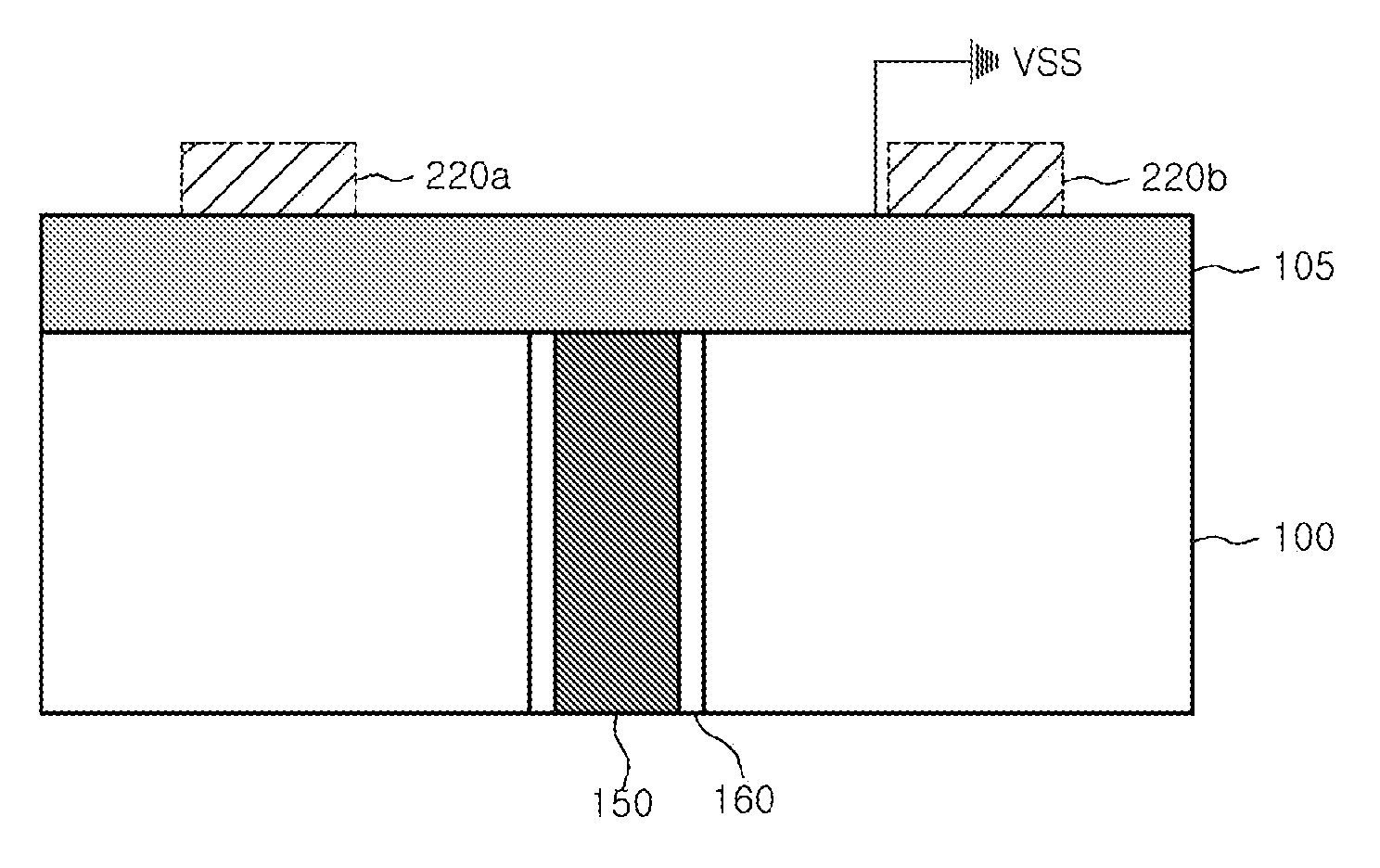
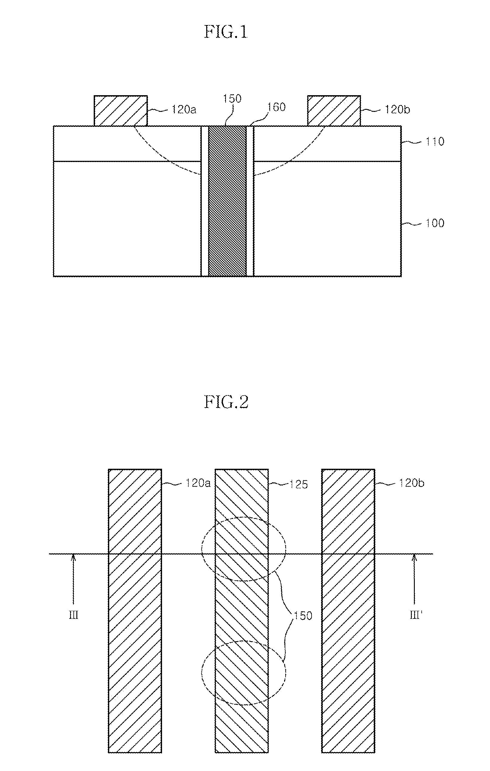
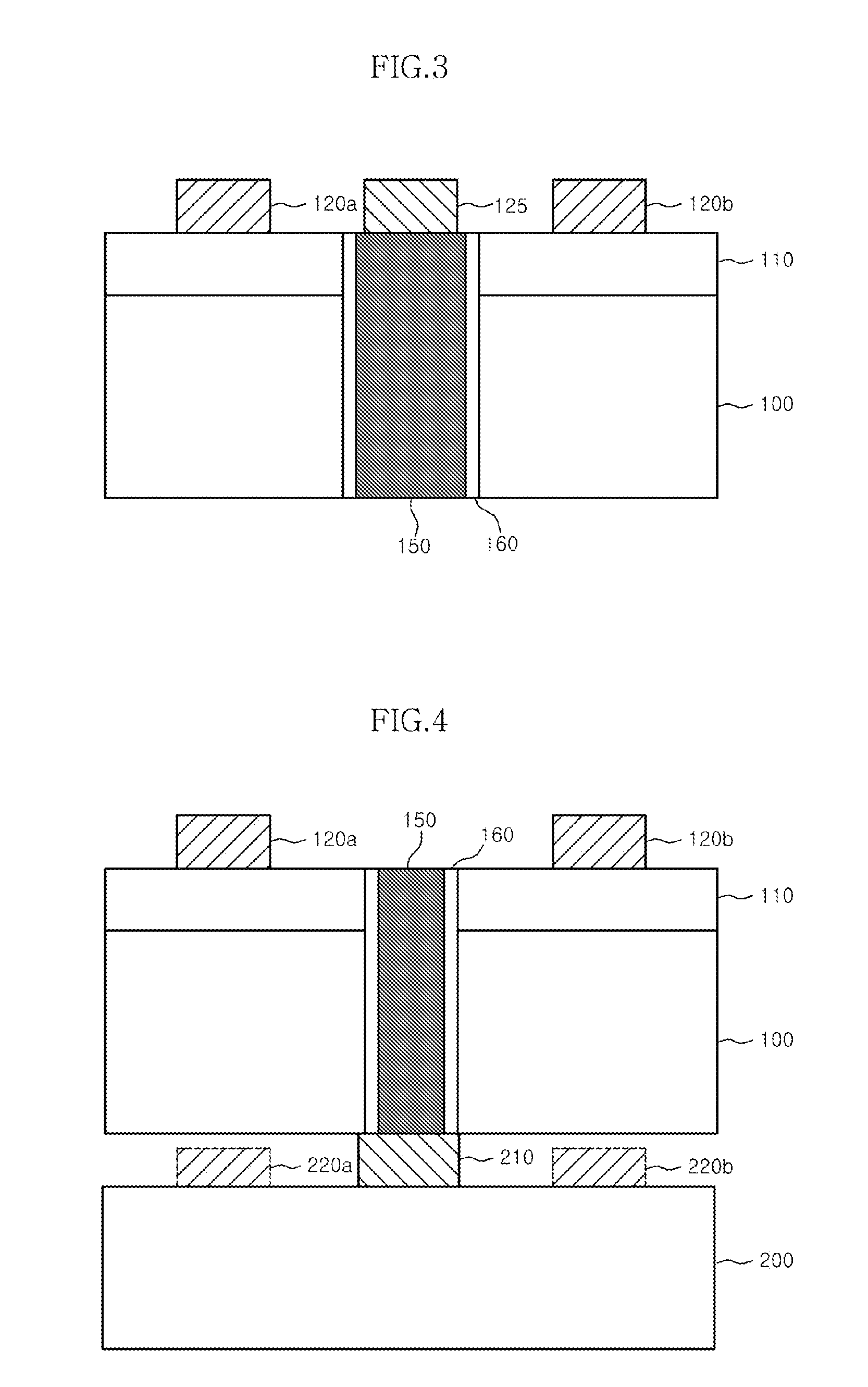
[0022]FIG. 1 is a cross-sectional view of a semiconductor integrated circuit apparatus according to an exemplary embodiment of the present inv...


PUM


Abstract

A semiconductor integrated circuit apparatus includes a semiconductor substrate, a plurality of signal lines, and at least one interface member. The signal lines are disposed on the semiconductor substrate. The interface member is disposed in the semiconductor substrate between the adjacent signal lines among the signal lines to pierce the semiconductor substrate.

Description

CROSS-REFERENCES TO RELATED APPLICATION[0001]The present application claims priority under 35 U.S.C. §119(a) to Korean application number 10-2011-0027581, filed on Mar. 28, 2011 in the Korean Intellectual Property Office, and which is incorporated herein by reference in its entirety.BACKGROUND[0002]1. Technical Field[0003]The present invention relates to a semiconductor integrated circuit apparatus, and more particularly, to a semiconductor integrated circuit apparatus including a shielding structure for preventing crosstalk between signal lines.[0004]2. Related Art[0005]As the integration density of semiconductor integrated circuit apparatuses increases, the distance between signal lines decreases. A decrease in the distance between signal lines causes crosstalk due to coupling noise between the signal lines, thus making it difficult to transmit an accurate signal.[0006]A method of forming a shielding line for preventing crosstalk between adjacent signal lines has been proposed to ...

Claims


Application Information

Patent Timeline
IPC IPC(8): H01L23/58H01L23/48
CPCH01L23/481H01L23/5222H01L23/552H01L24/16H01L25/0657H01L2225/06513H01L2225/06541H01L2224/16146H01L2924/00013H01L2224/13099H01L2224/13599H01L2224/05599H01L2224/05099H01L2224/29099H01L2224/29599H01L23/58
Inventor LEE, JUN HOKIM, HYUN SEOKJUNG, BOO HOCHO, SUN KIKIM, YANG HEEKIM, YOUNG WON
Owner SK HYNIX INC
Why Eureka
Try Eureka