CMOS image sensor and manufacturing method thereof

Inactive Publication Date: 2007-05-03
DONGBU ELECTRONICS CO LTD
View PDF4 Cites 3 Cited by
  • Summary
  • Abstract
  • Description
  • Claims
  • Application Information

AI Technical Summary

Benefits of technology

[0020] An object of the present invention is to provide a CMOS image sensor for preventing crosstalk by blocking light incident to adjacent pixels.

Problems solved by technology

However, the CMOS image sensor according to the related art has a following problem.
Crosstalk is a phenomenon causing a data error by light incident to an undesired pixel.

Method used


Image

  • CMOS image sensor and manufacturing method thereof
  • CMOS image sensor and manufacturing method thereof
  • CMOS image sensor and manufacturing method thereof

Examples


Embodiment Construction

[0032] Reference will now be made in detail to the preferred embodiments of the present invention, examples of which are illustrated in the accompanying drawings. Wherever possible, the same reference numbers will be used throughout the drawings to refer to the same or like parts.

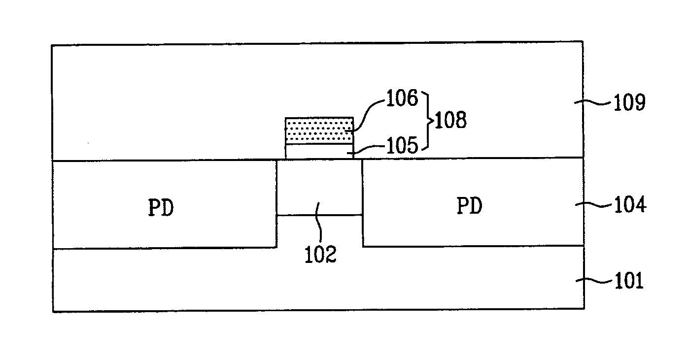
[0033]FIG. 4 is a plan view of a CMOS image sensor according to an embodiment of the present invention, and FIG. 5 is a cross-sectional view of the CMOS image sensor of FIG. 4 taken along the line V-V.

[0034] As shown in FIGS. 4 and 5, the CMOS image sensor according to an embodiment includes a plurality of photodiodes 104 formed on a semiconductor substrate 101 separated a predetermined distance from one another, a device isolation layer 102 formed between each of the photodiodes 104 in the semiconductor substrate 101, a light blocking layer 108 for blocking light incident one photodiode 104 from reaching an adjacent photodiode 104, and a dielectric layer 109 formed on the entire surface of the semiconduc...


PUM


Abstract

A CMOS image sensor and a method for manufacturing the same are provided. The method can include: forming a device isolation layer on a device isolation region of a semiconductor substrate; forming photodiodes on photodiode regions of the semiconductor substrate; forming a salicide metal layer and a barrier metal layer sequentially on the entire surface of the semiconductor layer; forming a light blocking layer between the photodiodes to block a light incident a photodiode from reaching an adjacent photodiode by selectively removing the salicide metal layer and the barrier metal layer that have not reacted during a silicide process; and forming a dielectric layer on the entire surface of the semiconductor substrate having the light blocking layer.

Description

RELATED APPLICATION [0001] This application claims the benefit under 35 U.S.C. §119(e) of Korean Patent Application Number 10-2005-0090454 filed Sep. 28, 2005, which is incorporated herein by reference in its entirety. FIELD OF THE INVENTION [0002] The present invention relates to a complementary metal oxide silicon (CMOS) image sensor, and more particularly, to a CMOS image sensor for preventing crosstalk by blocking light incident to adjacent pixels. BACKGROUND OF THE INVENTION [0003] In general, an image sensor is a semiconductor device that transforms an optical image to electrical signals. An image sensor is generally classified as a charge coupled device (CCD) or a CMOS image sensor. [0004] The CMOS image sensor is typically classified as a 3T type, a 4T type or a 5T type according to the number of transistors. The 3T type CMOS image sensor includes one photodiode and three transistors of a unit pixel, and the 4T type CMOS image sensor includes one photodiode and four transist...

Claims


Application Information

Patent Timeline
IPC IPC(8): H01L21/8238
CPCH01L27/14623H01L27/1463H01L27/146
Inventor JEON, IN GYUN
Owner DONGBU ELECTRONICS CO LTD
Why Eureka
Try Eureka