

Method of producing an ink-jet printing head
- Summary
- Abstract
- Description
- Claims
- Application Information
AI Technical Summary
Benefits of technology
Problems solved by technology
Method used
Image

Examples
sixth embodiments
Second to Sixth Embodiments
[0092]A list of other embodiments which are different from the first embodiment in structure is presented in Table 1 together with the first embodiment.
[0093]
TABLE 1PressureChannels inChamber WidthNo.UpperActiveand ActiveofOrienta-ElectrodeElementElement SideFig.tionPatterningSideWidth1FIG. 3(100)Photolitho-AnisotropicEqualgraphy AndWet EtchingEtching Steps2FIG. 5(100)LaserAnisotropicEqualProcessingWet Etching3FIG. 6(100)LaserDry EtchingEqualProcessing4FIG. 7(110)LaserAnisotropicEqualProcessingWet Etching5FIG. 8(110)LaserDry EtchingEqualProcessing6FIG. 9(110)LaserDry EtchingPressureProcessingChamber >Active Element
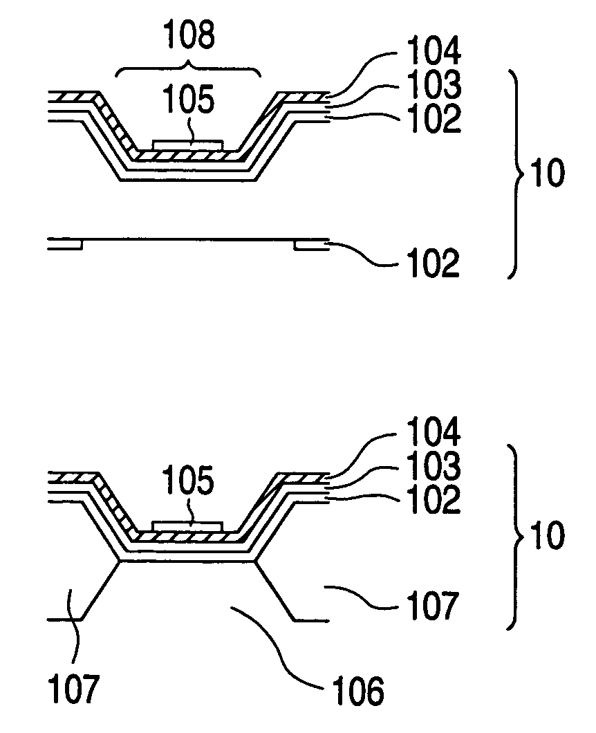
[0094]FIGS. 5 through 9 are cross-sectional views of pressurizing chamber substrates of the second through sixth embodiments which are taken along the plane perpendicular to the longitudinal direction of the pressurizing chamber. For brevity, as in FIGS. 5 to 9, only one of the pressurizing chambers is shown in these drawings.
[0095]FIG. 5 shows a...
first embodiment
of Manufacturing Method
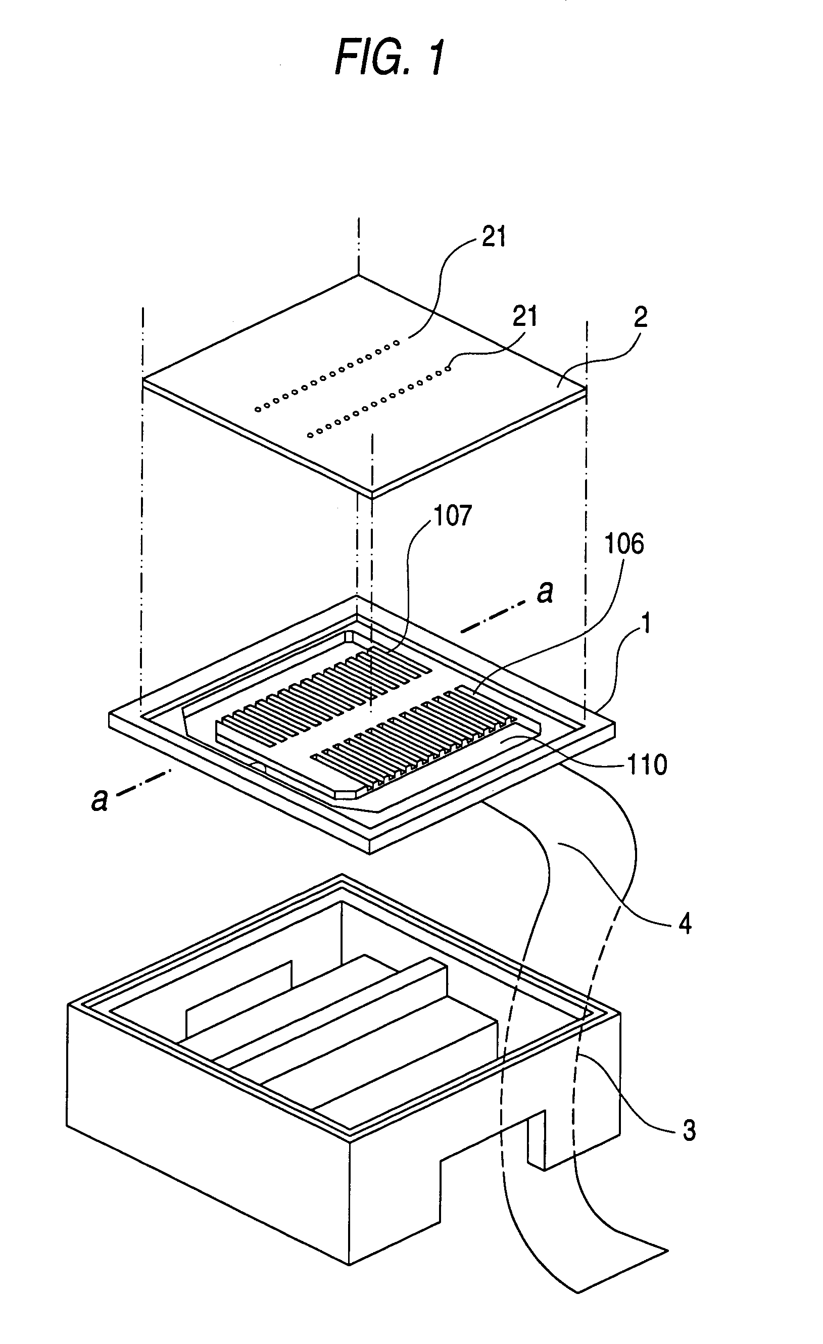
[0111]Next, an embodiment of the method of manufacturing the ink-jet printing head of the present aspect will be described.
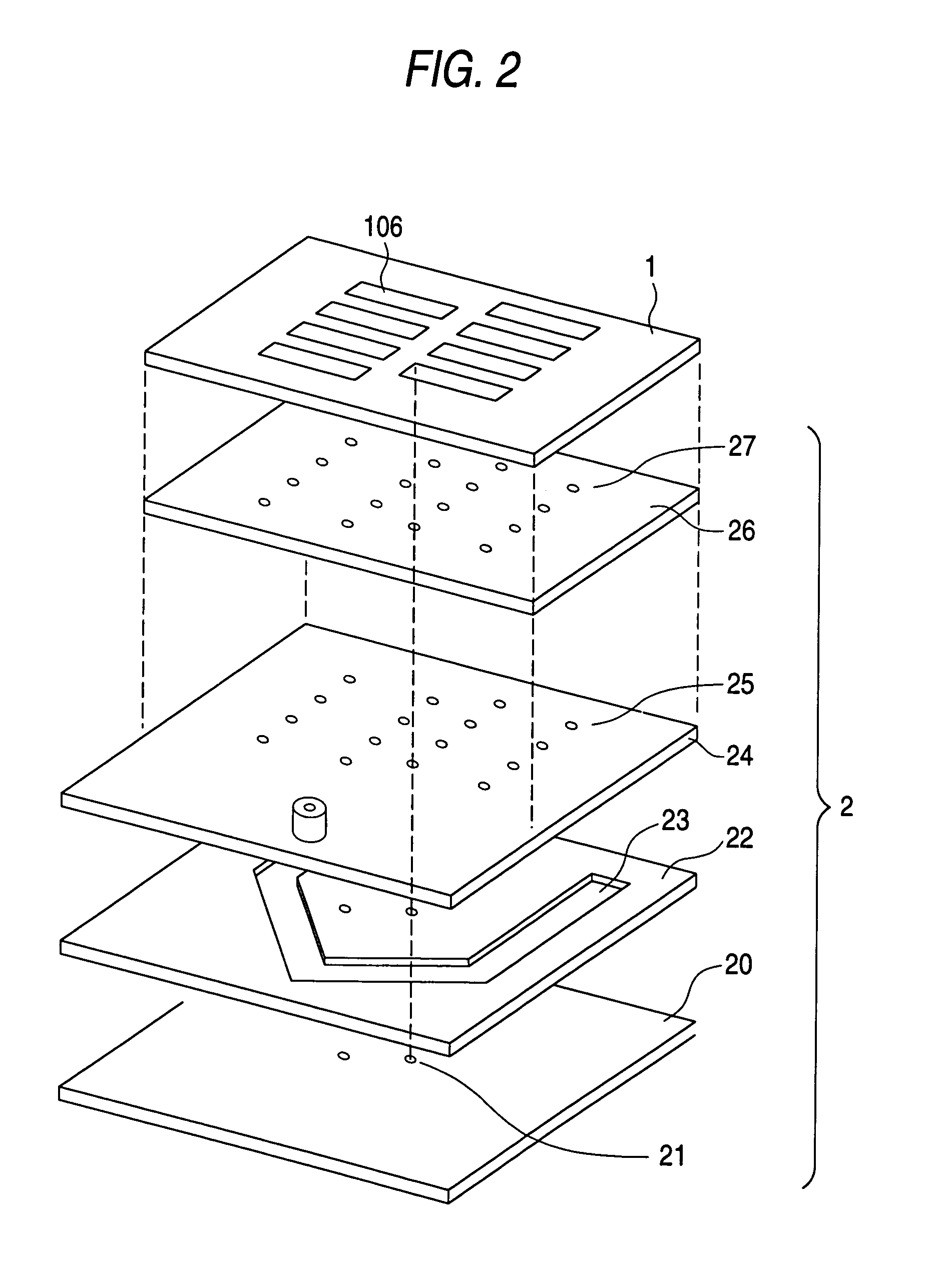
[0112]FIGS. 12A to 12E and FIGS. 13F to 13J show the cross section of the pressurizing chamber substrate of the present aspect during the course of the manufacturing steps. For brevity, the cross section of one of the pressurizing chamber substrates 1 formed on the silicon monocrystalline substrate 10 (a wafer) is schematically shown.
[0113]FIG. 12A: To being with, an etching protective layer 102 (a thermal oxide layer) comprising silicon dioxide is formed over the entire silicon monocrystalline substrate 10 having a (110) plane and predetermined thickness and size (e.g., a diameter of 100 mm and a thickness of 220 μm) by thermal oxidation.
[0114]The formation of the piezoelectric thin film can be considered to be the same as that in the first embodiment. In short, platinum which serves as the lower electrode 103 is formed on the surface of ...
second embodiment
(Second Embodiment of Manufacturing Method)
[0131]FIGS. 15F to 15I show a second embodiment of the manufacturing method for the ink-jet printing head. The previously described steps of the first embodiment shown in FIGS. 12A to 12E also apply to the present embodiment.
[0132]FIG. 15F: A mask is formed on the pressurizing chamber side of the substrate 10 in the shape in which the pressurizing chambers 106 are to be formed. The silicon dioxide film 102 that acts as an etching protective layer is etched by hydrogen fluoride. The areas of the etching protective layer 102 that correspond to the recesses 12 of the first embodiment are etched, so that thin-film areas 102a are formed.
[0133]FIG. 15G: The substrate 10 is further anisotropically etched from its pressurizing chamber side to active element side by use of anisotropic etchant; e.g., a water solution of potassium hydroxide having a concentration of about 17% as well as having its temperature maintained at a temperature of 80 degrees ...
PUM
| Property | Measurement | Unit |
|---|---|---|
| Thickness | aaaaa | aaaaa |
| Diameter | aaaaa | aaaaa |
| Mechanical strength | aaaaa | aaaaa |
Abstract
Description
Claims
Application Information