
Rf-id tag and rf-id communication system

a technology of radio frequency identification and communication system, which is applied in the structure of radiating elements, instruments, sensing details, etc., can solve the problems of lowering affecting the stability of product operation, and increasing the cost of communication, so as to reduce the cost of product operation, reduce the value of label expression, and increase the bandwidth of communication antennas.

Inactive Publication Date: 2012-10-04
FUJIFILM CORP
View PDF6 Cites 19 Cited by
  • Summary
  • Abstract
  • Description
  • Claims
  • Application Information

AI Technical Summary

Benefits of technology

[0006]In general, a one-turn loop antenna is connected to an IC chip and a booster antenna is disposed close to the coil of the 1-turn loop antenna in non-contact form. And the 1-turn loop antenna is disposed at the center of the booster antenna. Since the IC chip is disposed close to (for example, mounted on) the 1-turn loop antenna, the IC chip is located approximately at the center of the booster antenna. Therefore, in printing a label on an RF-ID tag, printing on a label central portion is avoided to prevent the IC chip (located in the label central portion) from being damaged. This restriction inevitably lowers the value of label expression.
[0008]A second object of the invention is to increase the degree of freedom of disposition of an IC chip by making it possible to dispose the IC chip at a position other than the center of a communication antenna.
[0015]The RF-ID tag and the RF-ID communication system according to the invention make it possible to provide a configuration for increasing the bandwidth of a communication antenna and thereby contribute to cost reduction and stabilization of product operation. Furthermore, disposing an IC chip at a position other than the center of a communication antenna prevents a disconnection from occurring in a connection portion of the IC chip and an antenna portion and eliminates restrictions relating to label printing to avoid lowering of the value of label expression.

Problems solved by technology

Because of the narrow resonance bandwidth, allowable variation ranges of performance items of components such as an IC chip and antenna members are narrow, which may increase the cost and affect the stability of product operation.
Furthermore, the resonance frequency may shift depending on the use situation such as interference between the communication antennas of adjoining RF-ID tags, which may disable a stable communication.
This restriction inevitably lowers the value of label expression.

Method used


Image

  • Rf-id tag and rf-id communication system
  • Rf-id tag and rf-id communication system
  • Rf-id tag and rf-id communication system

Examples


example 1

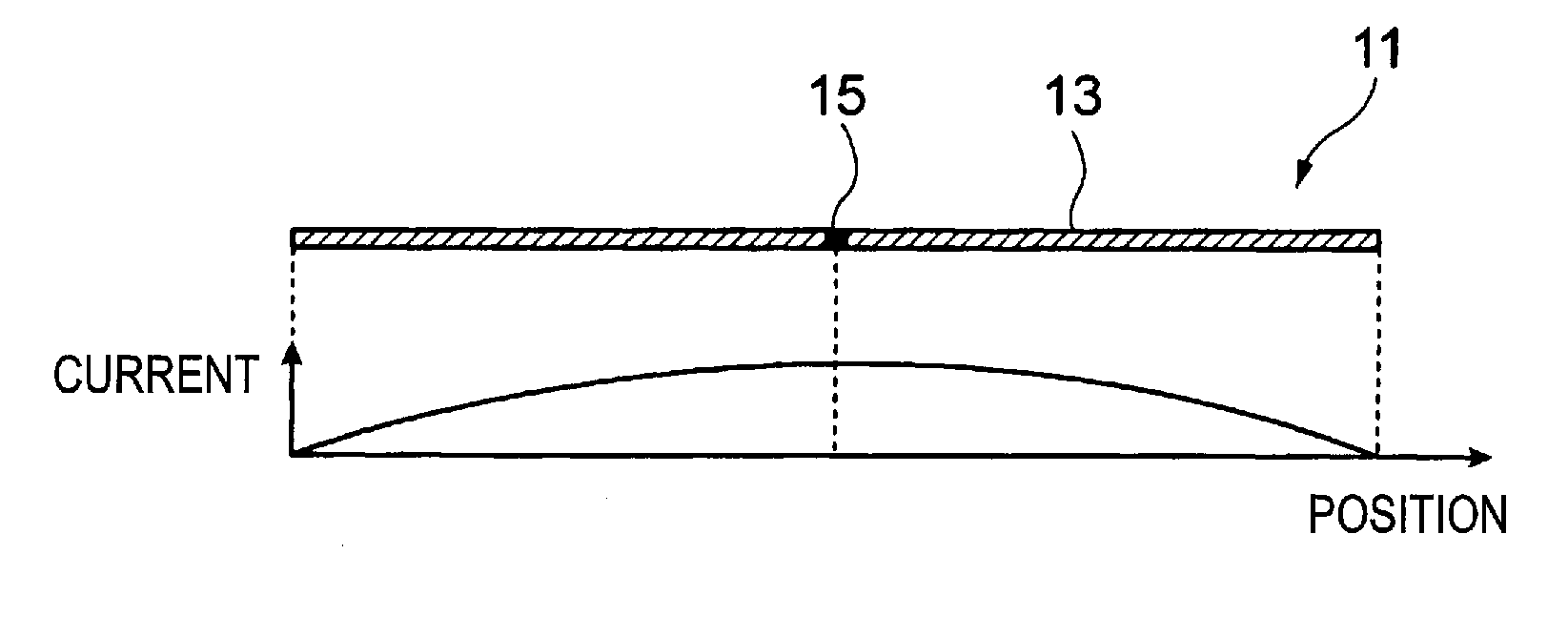
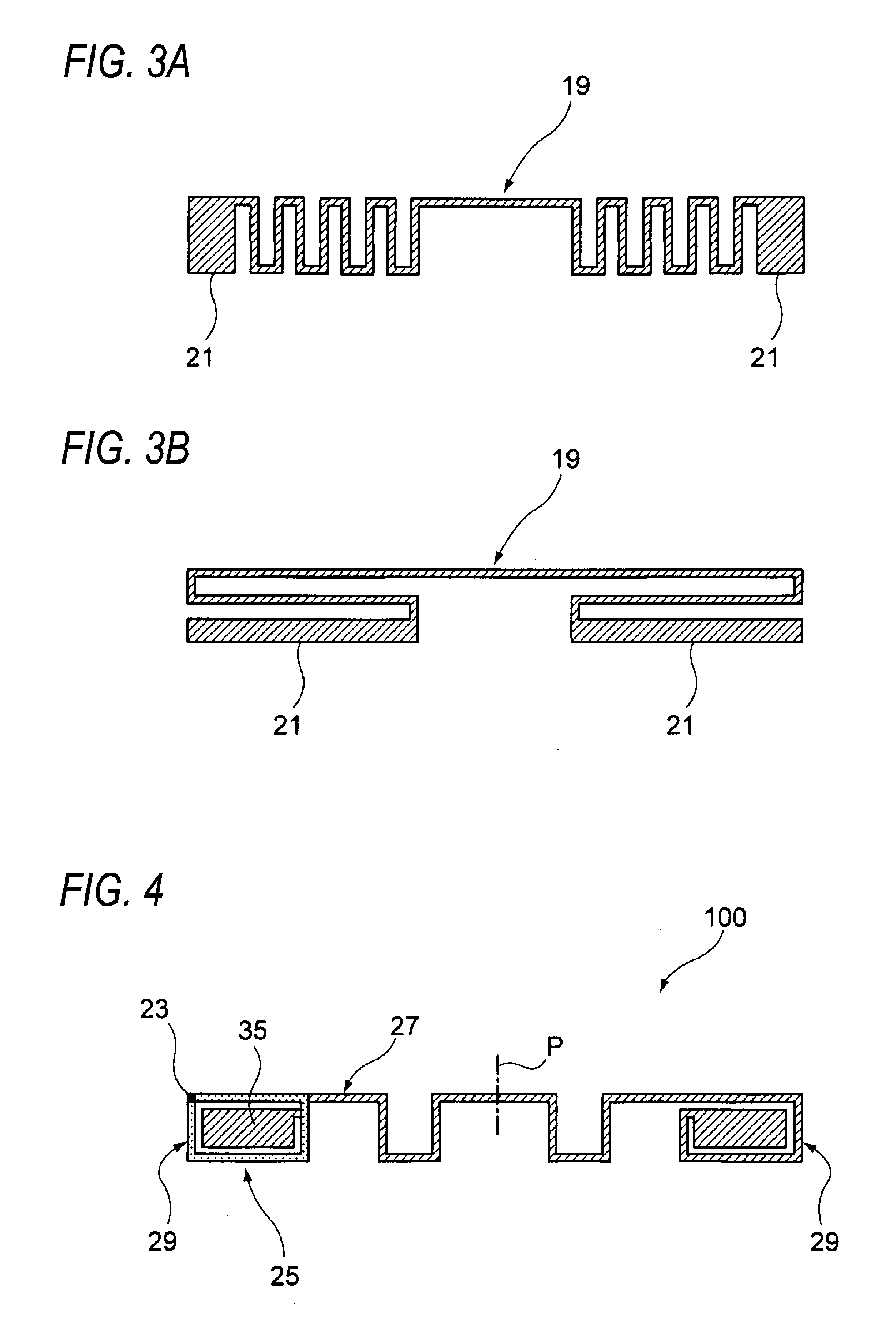
[0110]In a multilayer substrate, two layers having an arbitrary interval is provided as a loop antenna forming layer and a booster antenna forming layer. Which layers a loop antenna and a booster antenna should be formed in is determined as appropriate taking into consideration the thickness of each layer of the substrate, the permittivity of the substrate, and the antenna shapes.

example 2

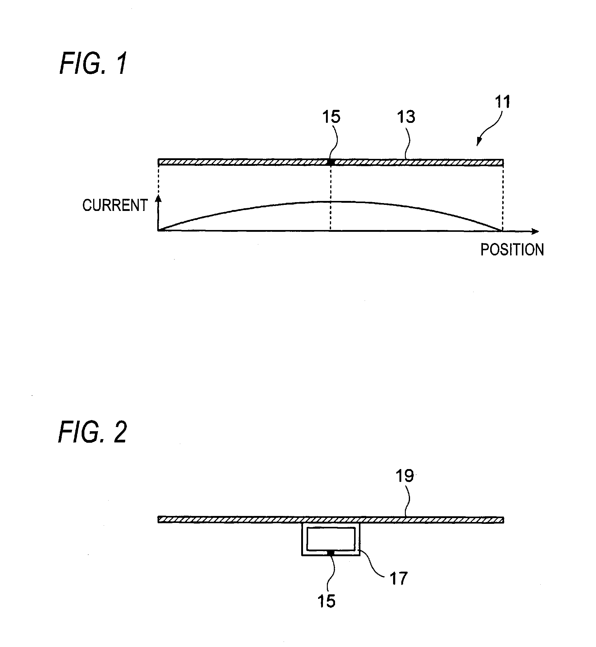
[0111]A loop antenna is formed on a substrate which includes a power source for an active tag. A booster antenna is disposed on the inner surface or the outer surface of an apparatus case which houses the substrate, so as have a particular positional relationship with a loop antenna.

[0112]Where as in the above examples the loop antenna and the booster antenna are separate from and not in contact with each other and have no wiring line connecting them, the booster antenna can be attached and removed when necessary according to a use and whether to permit long-distance communication (security function) or a like item can be set. In these examples, the one-turn loop antenna alone functions as a magnetic induction type tag.

[0113]Specific apparatus corresponding to the above Example 1 will be described below with reference to FIGS. 13 and 14.

[0114]FIG. 13 shows a recording tape cartridge 51 in which a magnetic tape T as an information recording medium is wound on a single reel 55 which i...


PUM


Abstract

An RF-ID tag has an IC, a loop antenna to which the IC is connected, and a linear booster antenna, and the booster antenna has, as one end portion in a longitudinal direction of the linear booster antenna, a fold-back portion which is wound; and a portion, having a length that measures 73% or more of a one-turn overall length of a loop of the loop antenna, of the loop antenna extends along a portion, including the fold-back portion, of the booster antenna.

Description

CROSS-REFERENCE TO RELATED APPLICATIONS[0001]This application claims the benefit of Japanese Patent Application JP 2011-081056, filed Mar. 31, 2011, the entire content of which is hereby incorporated by reference, the same as if set forth at length.FIELD OF THE INVENTION[0002]The present invention relates to an RF-ID (radio frequency identification) tag and an RF-ID communication system.BACKGROUND OF THE INVENTION[0003]In recent years, non-contact communication devices which receive information from the outside and send information to the outside using electromagnetic waves as a medium have come to be used commonly (refer to JP-A-2006-203852 and JP-A-2009-075687, for example). A non-contact IC label and a non-contact card which are example non-contact communication devices are equipped with an IC chip and a communication antenna that is electrically connected to the IC chip. When the communication antenna receives electromagnetic waves, electromotive force occurs in the communicatio...

Claims


Application Information

Patent Timeline
Patent Type & Authority Applications(United States)
IPC IPC(8): G06K7/01G06K19/077
CPCG06K19/07767G06K19/07783G06K19/07786G06K19/0779H01Q19/22H01Q1/2225H01Q1/38H01Q7/00G06K19/07794
Inventor TADA, NOBUYUKI
Owner FUJIFILM CORP
Learn More