Touch panel and touch-sensitive display device

a display device and touch panel technology, applied in the direction of dielectric materials, printed circuit aspects, instruments, etc., can solve the problems of high cost, difficult to form a curvy surface and the scrapping of a transparent conductive substrate with a touch panel, so as to improve the production yield, reduce material and production costs, and simplify the lamination procedure

Inactive Publication Date: 2012-10-04
WINTEK CORP
View PDF5 Cites 86 Cited by
  • Summary
  • Abstract
  • Description
  • Claims
  • Application Information

AI Technical Summary

Benefits of technology

[0005]To improve the remaining drawbacks of the prior arts, the primary objective of the present disclosure is to provide a touch panel structure and its manufacturing method, which forms a touch-panel conductor structure layer on a bonding layer to be joined to a planar or curvy panel of arbitrary curvature, so as to lower the material and production costs, improve the production yield, and simplify the panel lamination procedures in the manufacturing process, and, furthermore, to facilitate design of a thinner product.

Problems solved by technology

Generally the transparent conductive substrate is composed of glass or plastic, and is expensive.
Once a touch panel in the fabrication process fails, the transparent conductive substrate will be scrapped with the touch panel and cannot be recycled any more.
It is difficult also for a transparent conductive substrate to be formed as a curvy surface.
The assembling process is complex and tends to decrease yield and to increase the whole thickness of a touch panel.
This process is difficult and even need to be outsourced to the Original Equipment Manufacturer (OEM).

Method used


Image

  • Touch panel and touch-sensitive display device
  • Touch panel and touch-sensitive display device
  • Touch panel and touch-sensitive display device

Examples


first embodiment

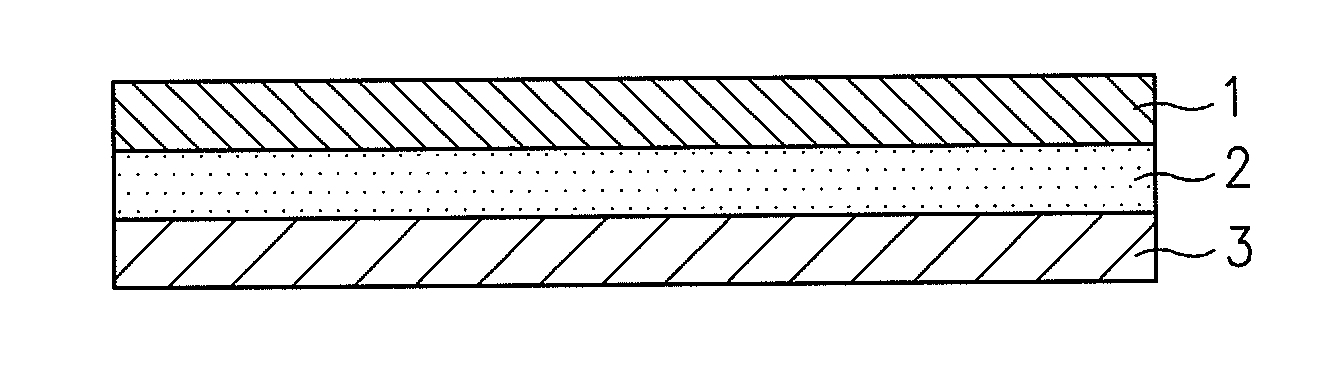
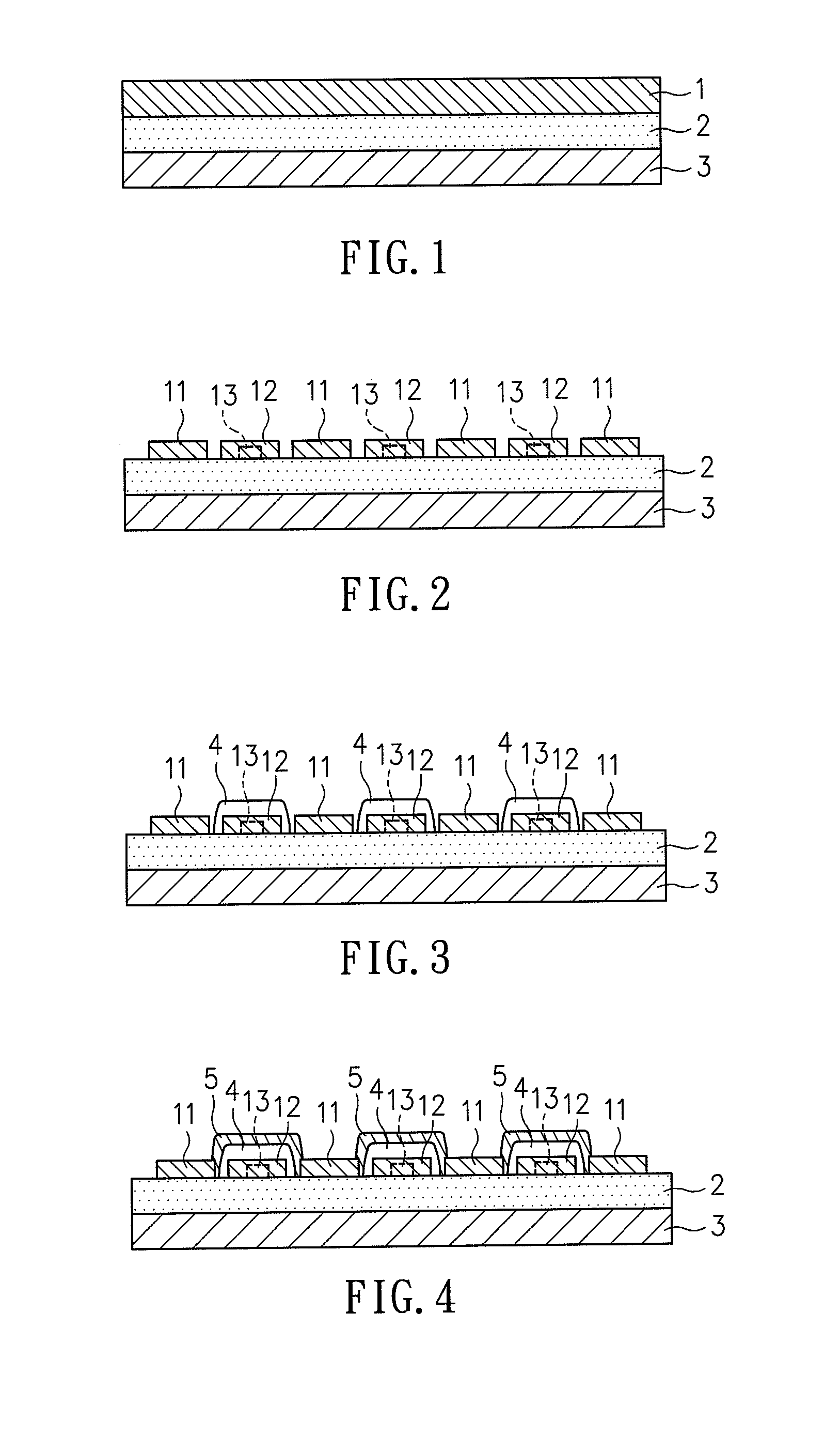
[0035]FIGS. 1 to 7 schematically illustrate evolutionary steps of fabrication process of a single-panel touch panel structure according to the present invention. Referring to FIG. 1, a transparent conductive layer 1 is formed on upper side of a bonding layer 2, which is composed of transparent photo-curing adhesive. A temporary base film 3 is joined to the lower side of the bonding layer 2. The transparent conductive layer 1 is patterned by means of the wet or dry etching process to form a plurality of first major conductors 11, a plurality of second major conductors 12, and a plurality of second conductive wires 13, wherein each of the first major conductors 11 alternates with each of the second major conductors 12, and the second conductive wires 13 are connected with the second major conductors 12, as shown in FIG. 2. On the second conductive wires 13, an insulation layer 4 is formed by means of the ink-jet printing, screen-printing, physical vapor deposition (PVD), or chemical v...

second embodiment

[0050]As to a double-panel touch panel, FIGS. 13 to 20 schematically illustrate evolutionary steps of fabrication process according to the present invention. Referring to FIG. 13, a transparent conductive layer la is formed on upper side of a bonding layer 2a, which is composed of transparent photo-curing adhesive. A temporary base film 3a is joined to the lower side of the bonding layer 2a. The transparent conductive layer la is patterned by the wet or dry etching to form a plurality of first major conductors 11a. Between any two adjacent first major conductor elements, a first conductive wire 12a is formed by means of the ink-jet printing, screen-printing, PVD or CVD, as shown in FIG. 14. On edges of the bonding layer 2a, a plurality of first conductive routing leads 6a are formed by means of the ink-jet printing, screen-printing, PVD, or CVD, to connect electrically the first major conductors 11a, as shown in FIG. 15. Thus, the first major conductors 11a, the first conductive wir...


PUM


Abstract

A touch panel structure and the manufacturing method thereof are disclosed, in which the manufacturing method includes the steps of: providing a bonding layer; and forming a conductive pattern layer on the bonding layer; wherein the conductive pattern layer is composed of at least one first and at least one second major conductors with an insulation layer interposed between the first and the second major conductors. Comparing with the prior art for manufacturing touch panels, the disclosure is advantageous in material cost, production cost, and production yield; moreover, the panel lamination process can be simplified and the touch panel structure can be joined to a planar or curvy panel and facilitate the design of a thinner product.

Description

CROSS-REFERENCE TO RELATED APPLICATIONS[0001]This application is a continuation-in-part of application Ser. No. 13 / 045,105, filed on Mar. 10, 2011.TECHNICAL FIELD[0002]The present invention relates to a touch panel structure, a touch-sensitive display device and the manufacturing method thereof, and more particularly, to a touch panel structure formed on a bonding layer, which can be joined to a panel of arbitrary curvature and simplifies manufacturing process of touch panel devices.TECHNICAL BACKGROUND[0003]Conventional touch panel structures, whether a single-panel or double-panel type, was fabricated by the screen-printing or photolithography process on a transparent conductive substrate. Generally the transparent conductive substrate is composed of glass or plastic, and is expensive. Once a touch panel in the fabrication process fails, the transparent conductive substrate will be scrapped with the touch panel and cannot be recycled any more. It is difficult also for a transparen...

Claims


Application Information

Patent Timeline
Patent Type & Authority Applications(United States)
IPC IPC(8): G06F3/041
CPCG06F3/041G06F2203/04103H05K2201/10106H05K2201/09H05K2201/10128H05K1/0393H05K1/0306H05K1/0296H05K2201/017G06F3/0412G06F3/0445G06F3/0446G06F2203/04102
Inventor LIN, YI-CHUNWU, MING-KUNGLI, HSIAO-PINGHUANG, PING-WENCHOU, CHENG-YIWU, YU-HUASHIU, XUAN-CHANGWANG, CHIH-YUANHSU, CHING-FULIAO, SHIAO-HUICHANG, TING-YUWU, FA-CHENWANG, WEN-CHUN
Owner WINTEK CORP
Why Eureka
Try Eureka