Electronic component manufacturing method

a manufacturing method and electronic component technology, applied in the field of electronic component manufacturing methods, can solve the problems of lengthening the life of the rotary blade, and achieve the effect of efficient grinding and reduced thickness of electronic components

Active Publication Date: 2012-10-04
MURATA MFG CO LTD
View PDF12 Cites 6 Cited by
  • Summary
  • Abstract
  • Description
  • Claims
  • Application Information

AI Technical Summary

Benefits of technology

[0031]According to various preferred embodiments of the present invention, even when the substrate is warped, the cover layer provided on the substrate can be efficiently ground. Further, since grinding can be performed so that the thickness of the substrate rarely varies, the thickness of the electronic component can be decreased.

Problems solved by technology

This lengthens the life of the rotary blade, and can stably obtain a flat ground surface with few irregularities even through long-time grinding.

Method used


Image

  • Electronic component manufacturing method
  • Electronic component manufacturing method
  • Electronic component manufacturing method

Examples


first preferred embodiment

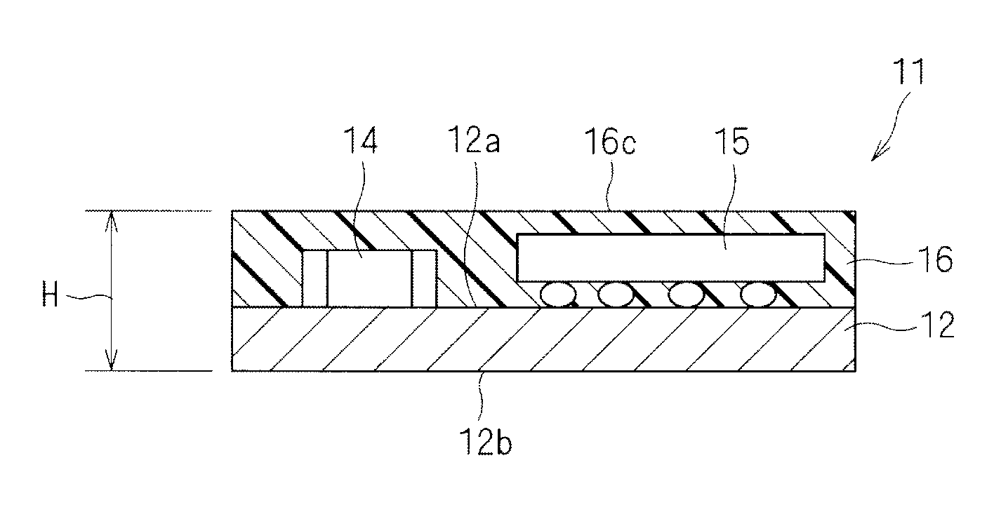
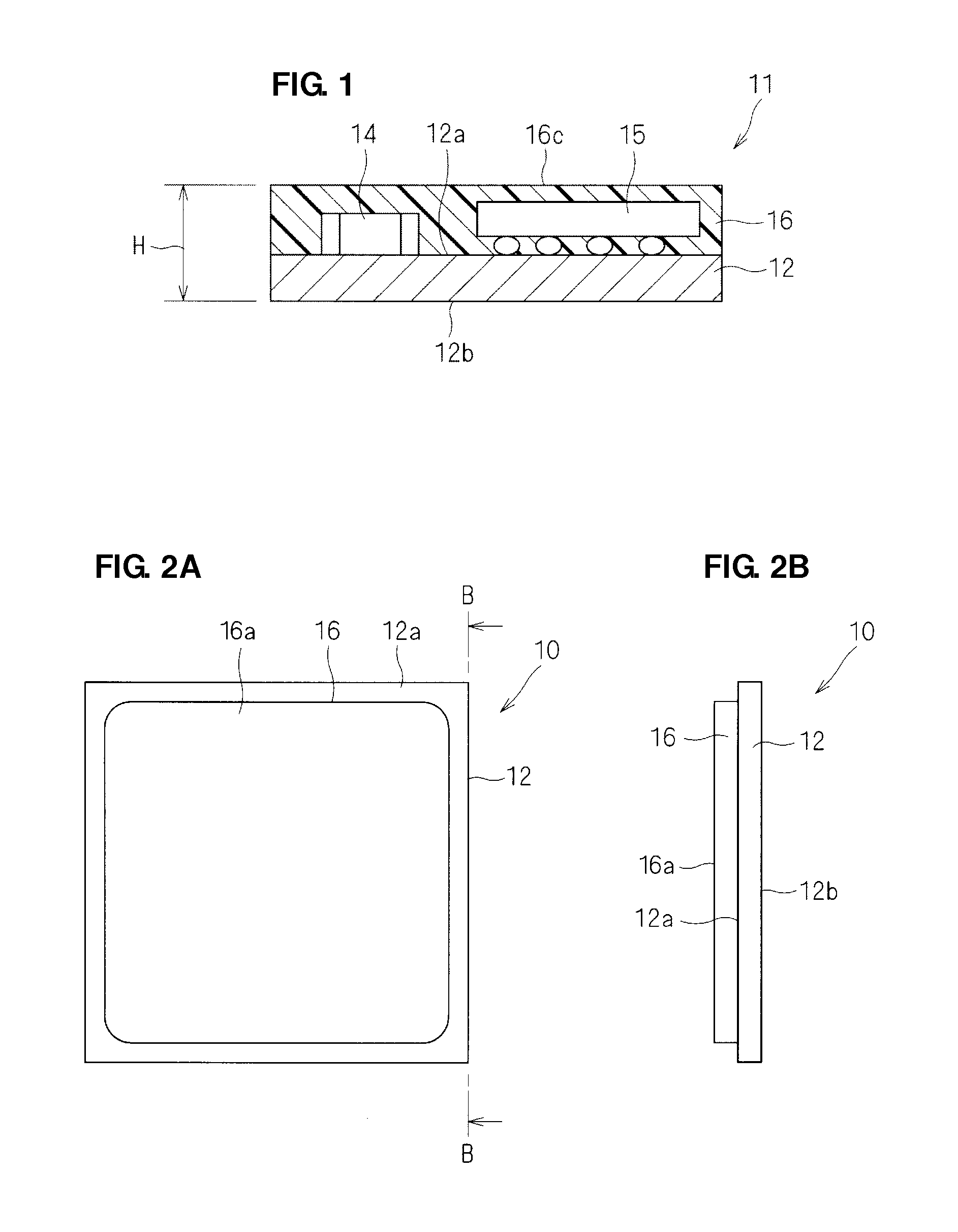
[0048]A manufacturing method for an electronic component 11 according to a first preferred embodiment will be described with reference to FIGS. 1 to 7 and FIGS. 13A and 13B.

[0049]In the electronic component 11, as illustrated in a cross-sectional view of FIG. 1, a cover layer 16 is provided on an upper surface 12a of a substrate 12. An upper surface 16c of the cover layer 16 is ground flat. Components 14 and 15, such as a chip component and a semiconductor chip, are mounted on the upper surface 12a of the substrate 12, and the components 14 and 15 are covered with the cover layer 16.

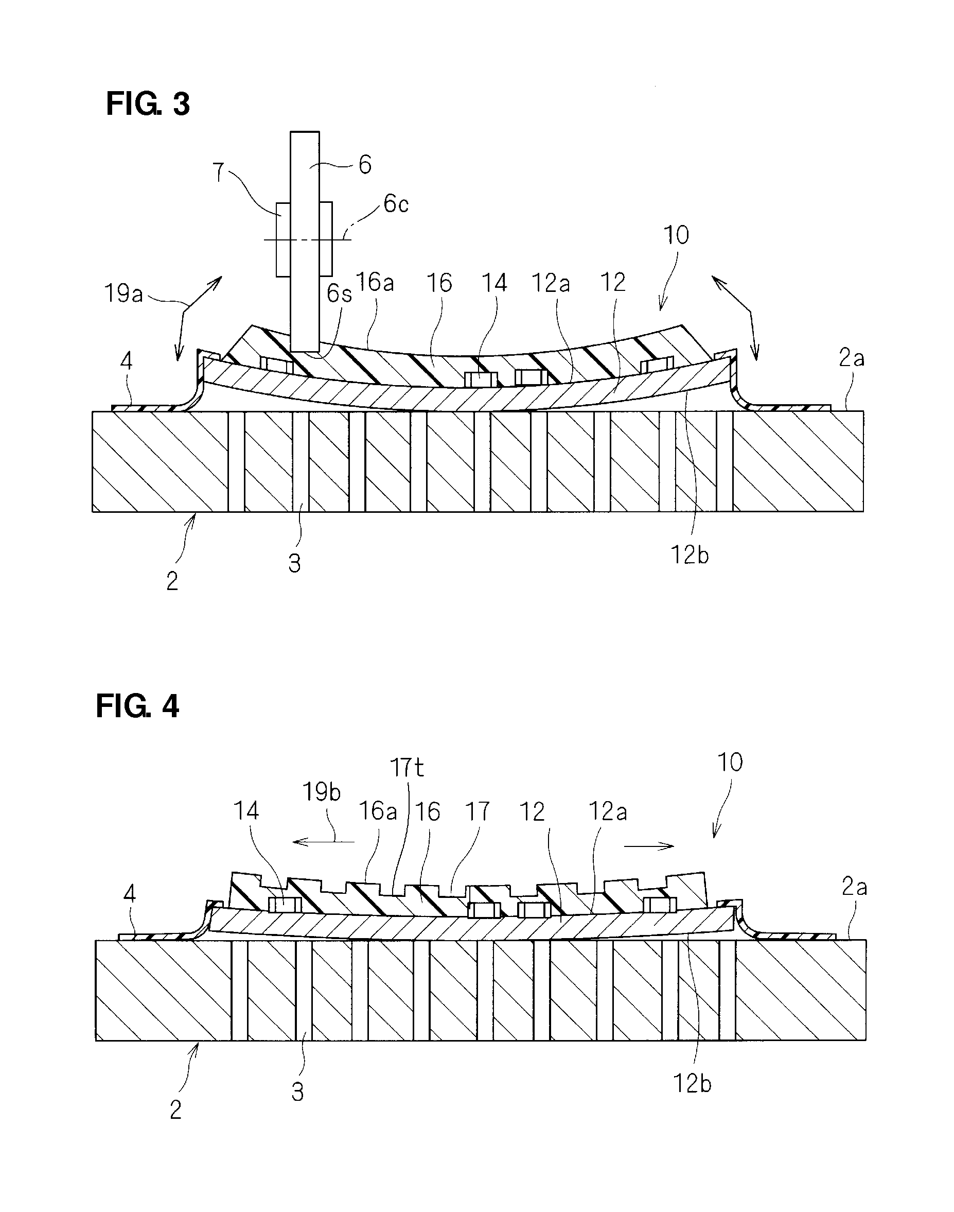
[0050]For example, the substrate 12 is a laminated body formed preferably by alternately stacking an insulator and a conductor. The substrate 12 in which the insulator is a resin or ceramic material easily warps when the cover layer 16 formed of resin or the like is formed. For this reason, it is highly effective to perform main grinding after preliminary grinding, as will be described below.

[0051]The el...

second preferred embodiment

[0086]An electronic component manufacturing method according to a second preferred embodiment will be described with reference to FIGS. 8A-9C.

[0087]An electronic component manufacturing method of the second preferred embodiment preferably is almost the same as the electronic component manufacturing method of the first preferred embodiment. The second preferred embodiment preferably is different only in that preliminary grinding is performed only once in contrast to the first preferred embodiment in which preliminary grinding is performed twice, but is the same in other aspects. Hereinafter, the same constituents as those in the first preferred embodiment are denoted by the same reference numerals, and a description will be given with a focus on differences from the first preferred embodiment.

[0088]In the electronic component manufacturing method of the second preferred embodiment, preliminary grinding is performed only once, as illustrated in FIGS. 8A-8D. FIG. 8A is a plan view sche...


PUM

PropertyMeasurementUnit
widthaaaaaaaaaa
thicknessaaaaaaaaaa
lengthaaaaaaaaaa

Abstract

An electronic component manufacturing method that efficiently grinds a cover layer provided on a substrate even when the substrate is warped includes the step of forming first grooves at intervals in a cover layer provided on a substrate by repeating grinding with a rotary blade at a pitch more than a thickness W of the rotary blade. Next, at least portions provided in the cover layer along the first grooves are removed to reduce the thickness of the cover layer by repeating grinding at a pitch equal to or less than the thickness W of the rotary blade.

Description

BACKGROUND OF THE INVENTION[0001]1. Field of the Invention[0002]The present invention relates to an electronic component manufacturing method, and more specifically, to a manufacturing method for an electronic component in which a cover layer formed of resin or the like is provided on a substrate.[0003]2. Description of the Related Art[0004]An electronic component in which a cover layer is provided on a substrate has been proposed. For example, such an electronic component is produced through steps illustrated in cross-sectional views of FIGS. 14A-14E.[0005]That is, semiconductor chips 139 are mounted on a substrate 130, and resin 152 in a liquid form is dropped from a dispenser 151 and is then cured to cover the semiconductor chips 139. Since the height of a surface of the resin 152 sometimes differs between the center and the periphery or is not equal to a predetermined height, the surface of the resin 152 is ground with a dicing blade 154 so that the height of the surface of the ...

Claims


Application Information

Patent Timeline
Patent Type & Authority Applications(United States)
IPC IPC(8): B24B1/00B32B3/30B24B41/06
CPCH01L21/56Y10T428/24612H01L23/24H01L23/3121H01L23/562H01L24/97H01L2224/16225H01L2924/01004H01L2924/1815H01L2924/19105B24B19/028B24B7/228H01L2924/01005H01L2924/01006H01L2924/01033H01L2924/01074B32B3/30H01L21/67092H01L2924/12042H01L2924/3511Y10T428/2457H01L2924/00
Inventor KAWAI, HIDEMASA
Owner MURATA MFG CO LTD
Why Eureka
Try Eureka