

Methods of manufacturing mask blank and transfer mask
a mask blank and mask technology, applied in the field of mask blanks and mask masks, can solve the problems that the expected cd accuracy cannot be obtained, and achieve the effects of preventing the charge-up of the mask blank, efficient grounding, and reducing the influence of the resist resolution
Active Publication Date: 2010-02-02
HOYA CORP
View PDF5 Cites 1 Cited by
- Summary
- Abstract
- Description
- Claims
- Application Information
AI Technical Summary
Benefits of technology
The patent text discusses the problem of forming a fine pattern in semiconductor devices using immersion exposure with a high numerical aperture (NA) of 45 nm and beyond. The issue is caused by the influence of mask blank charge-up, which affects the resolution of the resist pattern. The text proposes a solution to efficiently ground the mask blank on the stage of an exposure apparatus to prevent charge-up and improve pattern accuracy. However, the use of a shielding plate to prevent charge-up may narrow the film forming region of the etching mask film and lead to a lack of alignment mark pattern. The technical effect of this invention is to provide a method for efficiently grounding the mask blank to prevent charge-up and improve pattern accuracy while ensuring the alignment mark pattern is not compromised.
Problems solved by technology
However, it has been found that there is a problem in that the expected CD accuracy cannot be obtained by employing the immersion exposure with NA>1 to form a fine pattern according to the semiconductor design rule of DRAM half-pitch (hp) 45 nm (hereinafter referred to as “hp45 nm”) and onward.
Method used
View moreImage
Smart ImageViewing Examples

Examples
example 2
[0081]Example 2 was the same as Example 1 except that an inorganic-based etching mask film 3 was made of SiON instead of MoSiN.
[0082]The results of the evaluation were the same as those of Example 1.
Login to View More PUM
| Property | Measurement | Unit |
|---|---|---|
| size | aaaaa | aaaaa |
| width | aaaaa | aaaaa |
| refractive index | aaaaa | aaaaa |
Abstract
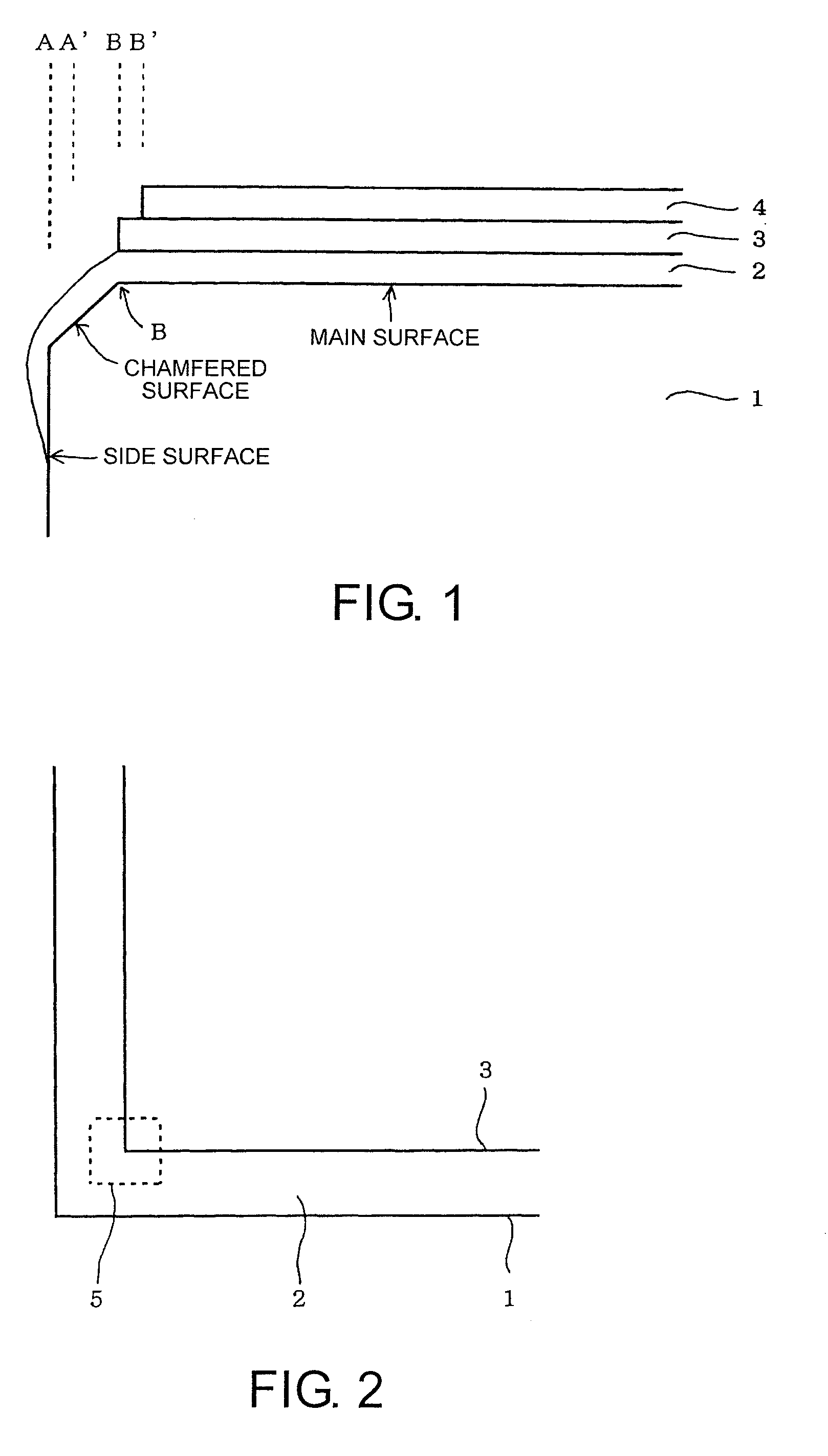
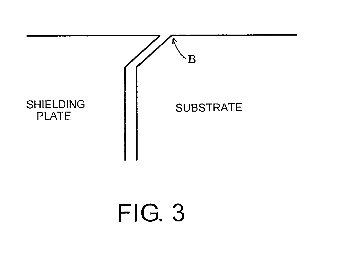
In a method of manufacturing a mask blank adapted to be formed with a resist pattern by electron beam writing and having a light-shielding film and an etching mask film of an inorganic-based material resistant to etching of the light-shielding film which are formed in this order on a transparent substrate, when forming the etching mask film, shielding is performed using a shielding plate so as to prevent the etching mask film from being formed at least at a side surface of the substrate.
Description
[0001]This application is based upon and claims the benefit of priority from Japanese patent application JP 2007-287272, filed on Nov. 5, 2007, the disclosure of which is incorporated herein in its entirety by reference.TECHNICAL FIELD[0002]This invention relates to methods of manufacturing a mask blank and a transfer mask for use in manufacturing semiconductor devices, display devices (display panels), or the like.BACKGROUND ART[0003]The miniaturization of semiconductor devices and the like is advantageous in bringing about an improvement in performance and function (higher-speed operation, lower power consumption, etc.) and a reduction in cost and thus has been accelerated more and more. The lithography technique has been supporting this miniaturization and transfer masks are a key technique along with exposure apparatuses and resist materials.[0004]In recent years, use has been made of photomasks applied with the resolution enhancement technology (RET) such as the phase shift tec...
Claims
Login to View More Application Information
Patent Timeline
 Patent Type & AuthorityPatents(United States)
IPC IPC(8): G03F9/00G03F1/50G03F1/54
CPCB82Y10/00B82Y40/00G03F1/14G03F1/78G03F7/2063H01J37/3174G03F1/32Y10S430/143G03F1/50G03F1/62
InventorKOMINATO, ATSUSHISUZUKI, TOSHIYUKIOKUBO, YASUSHI
OwnerHOYA CORP