Scanning probe lithography apparatus and method, and material accordingly obtained

a probe lithography and scanning probe technology, applied in the direction of instruments, measurement devices, photomechanical treatment, etc., can solve the problems of high volume manufacturing, unfavorable writing times for e-beam mask/master fabrication, and low throughput of ml2

Inactive Publication Date: 2012-10-04
IBM CORP
View PDF8 Cites 3 Cited by
  • Summary
  • Abstract
  • Description
  • Claims
  • Application Information

AI Technical Summary

Problems solved by technology

However, when approaching high resolutions, writing times for e-beam mask / master fabrication increase unfavorably.
However, the low throughput of ML2 (compared to that of e.g. optical lithography) has excluded it from high volume manufacturing.
Its main drawback arises due to the low exposure throughput of single charged particle beams.
Although this has led to a major improvement in throughput, such a system does however not have a throughput that is competitive enough for applications in chip manufacturing.
In addition, for research and development, it suffers a lack of resolution and a high cost due to the required e-beam.
In addition, the stitching accuracy and the proximity effect between the exposures of two adjacent characters remains an issue.
However, even with massive parallelism, throughput is still a major issue for applications such as chip manufacturing.

Method used


Image

  • Scanning probe lithography apparatus and method, and material accordingly obtained
  • Scanning probe lithography apparatus and method, and material accordingly obtained
  • Scanning probe lithography apparatus and method, and material accordingly obtained

Examples


Embodiment Construction

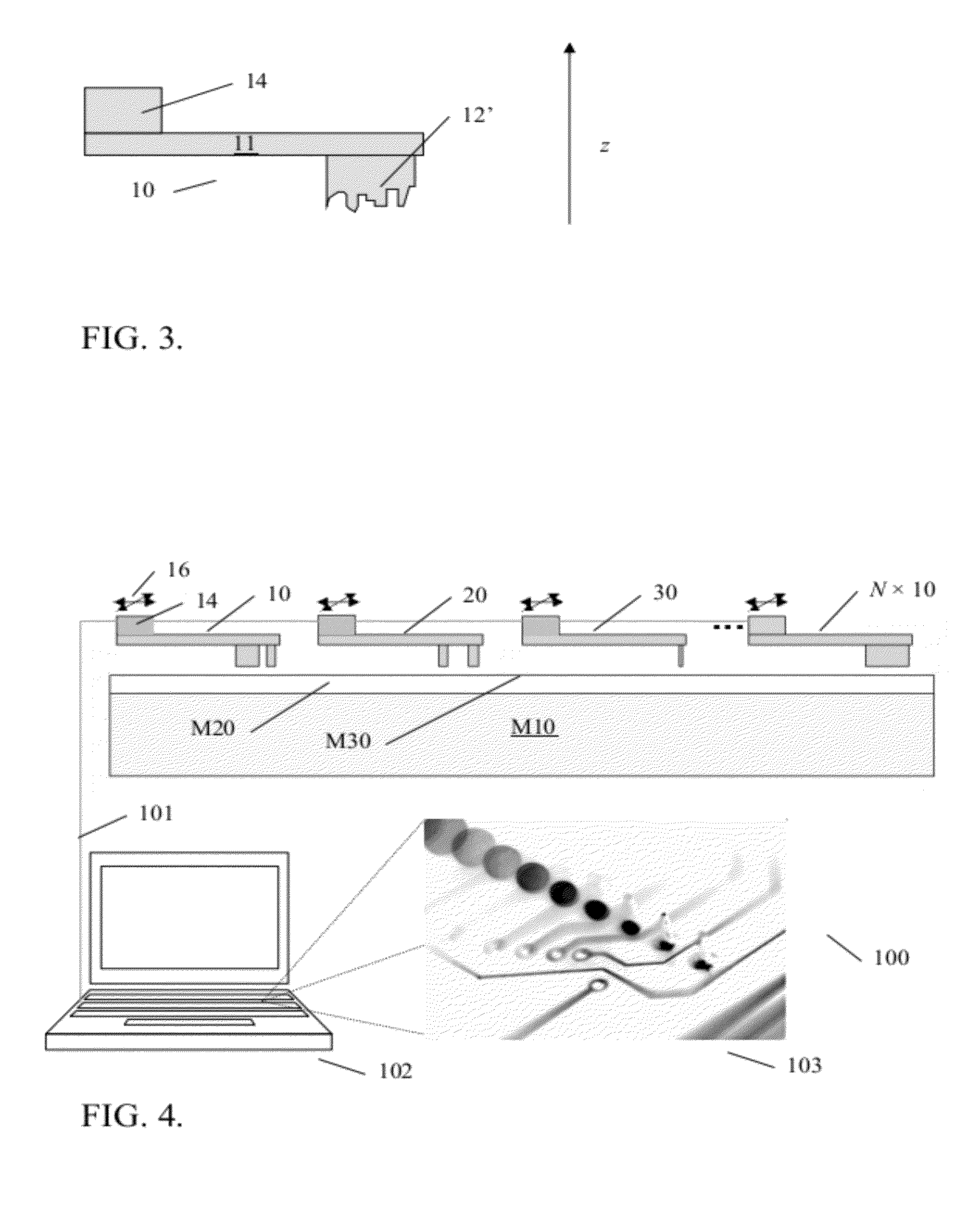
[0039]As an introduction to the following description, it is first pointed at general aspects of the invention, notably directed to a scanning probe lithography (or SPL) apparatus. The apparatus comprises physical probes with different shapes. The shapes actually differ such as to be able to form different patterns in the surface thickness of a material. Therefore, the diversity of patterns obtained during a raster scan of the material surface is increased. Typically, the idea is to use tips of specific shapes to imprint their shapes (or characters) in a polymer, whereby a complex structure can be created in one imprint step. Throughput of SPL is accordingly improved. Most advantageously, the probes are independently actuated, in order to further increase the diversity of patterns. Character probe lithography is thereby instated.

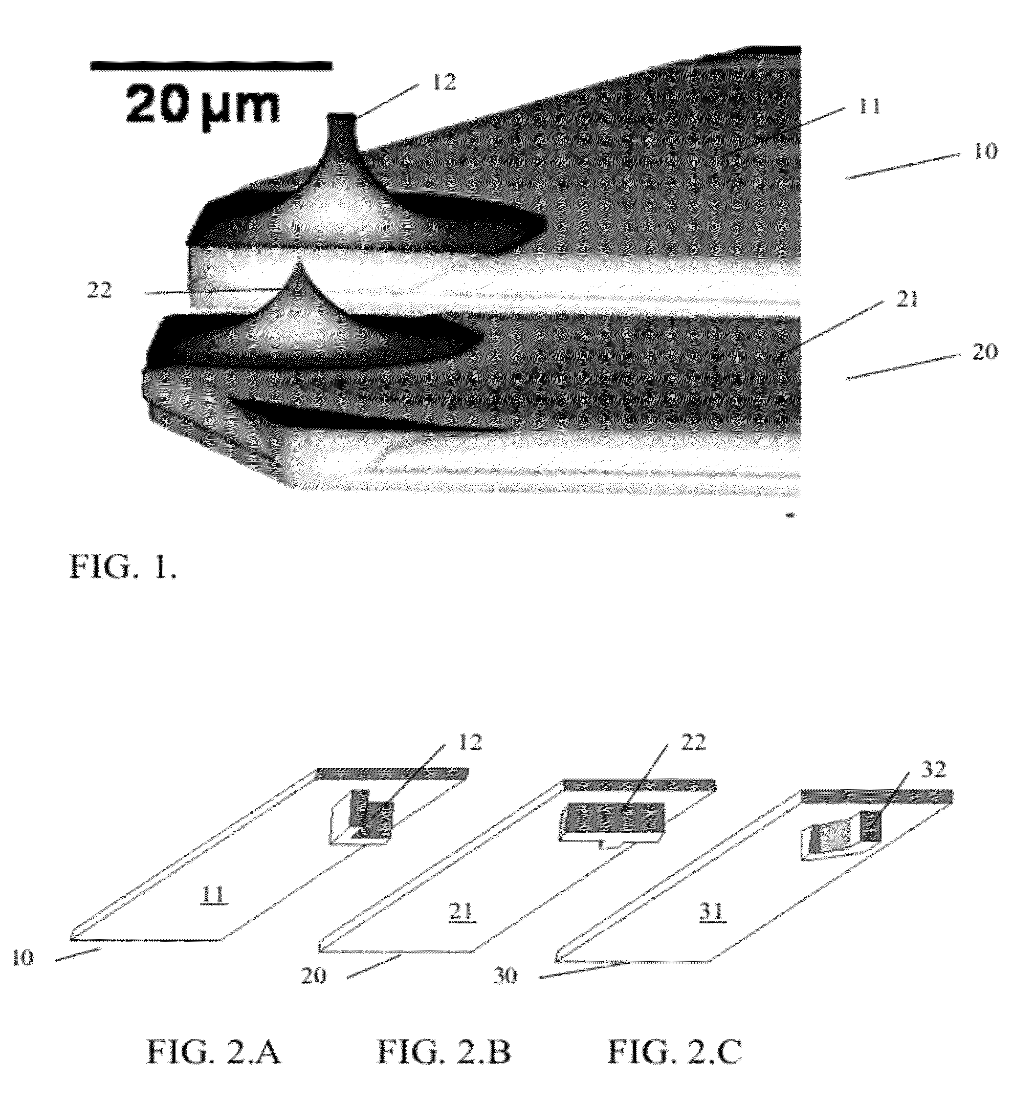
[0040]To prove the feasibility of the concept, FIG. 1 shows a picture representing an example of integration of two probes 10, 20, i.e. two cantilevers 11, ...


PUM


Abstract

A scanning probe lithography (SPL) apparatus, an SPL method, and a material having a surface thickness patterned according to the SPL method. The apparatus includes: two or more probes with respective shapes, where the respective shapes are different and the respective shapes form, in operation, different patterns in a thickness of a surface of a material processed with the apparatus.

Description

FIELD OF THE INVENTION[0001]The invention relates to the field of probe-based methods for patterning a surface of a material. In particular, it relates to scanning probe lithography (herein after SPL). It may furthermore be directed to high resolution / high throughput patterning, such as nano-scale patterns with feature sizes of e.g. less than 22 nanometers (nm).BACKGROUND OF THE INVENTION[0002]Lithography is a process for producing patterns of two dimensional shapes, consisting of drawing primitives such as lines and pixels within a layer of material, such as, for example, a resist coated on a semiconductor device.[0003]A conventional lithography is the photolithography or optical lithography. Many alternative approaches are known, for example in the field of nano lithography, which can be seen as high resolution patterning of surfaces. Nanolithography refers to fabrication techniques of nanometer-scale structures, comprising patterns having one dimension typically sizing up to abou...

Claims


Application Information

Patent Timeline
Patent Type & Authority Applications(United States)
IPC IPC(8): G01Q80/00G01Q70/10
CPCB82Y10/00G03F7/0002B82Y40/00
Inventor DESPONT, MICHELDUERIG, URS T.GOTSMANN, BERND W.KNOLL, ARMIN W.PIRES, DAVID SANTOSVETTIGER, PETER
Owner IBM CORP
Why Eureka
Try Eureka