Method for making circuit board
a technology of circuit board and fabrication method, which is applied in the field of making circuit board structure, can solve the problem of not providing more pins, and achieve the effect of increasing processing speed and simplifying the total structure and fabrication methods
- Summary
- Abstract
- Description
- Claims
- Application Information
AI Technical Summary
Benefits of technology
Problems solved by technology
Method used
Image
Examples
first embodiment
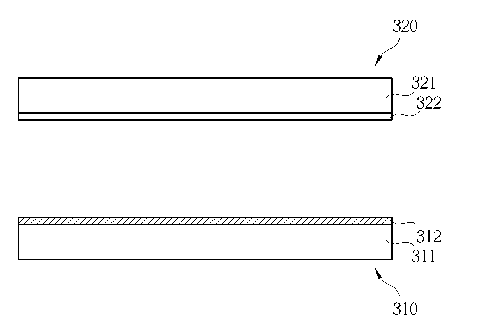
[0030]The present invention in a first aspect provides the method for making a circuit board structure. FIGS. 7-11 illustrate the method for making the circuit board structure of the present invention. Please refer to FIG. 7, initially a first substrate 310 and a second substrate 320 are provided. The first substrate 310 and the second substrate 320 may be prepared separately. They can be laminated together to form a single substrate (not shown) when needed. The first substrate 310 includes a carrier 311, and a release film 312 which is attached to one side of the carrier 311. The second substrate 320 includes a copper film 321 with a thickness of about 10 μm-70 μm, preferably 10 μm-35 μm. Only one side of the copper film 321 is covered with a solder mask 322.
[0031]The carrier 311 may be any suitable material, such as polyethylene terephthalate (PET), polycarbonate (PC), polymethylmethacrylate (PMMA) or a copperless substrate. The release film 312 may be a plastic and sticky materia...
second embodiment
[0035]In the present invention for making a circuit board structure as shown in FIG. 10A, a covering solder mask 327 may be optionally formed to completely cover the first pattern 325, the die pad 328 and the second pattern 326. The covering solder mask 327 may serve as a protection layer of the second pattern 326 to be followed with, please refer to FIG. 10B, the covering solder mask 327 is patterned to expose the needed element (s). For example, the covering solder mask 327 is patterned to expose the first pattern 325, the die pad 328 and to cover the second pattern 326 so the covering solder mask 327 may serve as the protection layer of the second pattern 326.
[0036]Afterwards, as shown in FIG. 11 a first passivation layer 323 should be formed on the surface of the copper film 321 in order to protect the fragile copper film 321. Because there are the first pattern 325 and the second pattern 326 of different functions on the patterned copper film 321, the first passivation layer 32...
PUM
| Property | Measurement | Unit |
|---|---|---|
| time | aaaaa | aaaaa |
| size | aaaaa | aaaaa |
| speed | aaaaa | aaaaa |
Abstract
Description
Claims
Application Information


