MEMS package

a technology of mems and packaging, applied in the field of mems packages, can solve the problems of insufficient electromagnetic interference of the converted signal, complicated packaging process, etc., and achieve the effects of improving damping characteristics, reducing the volume of the first cavity, and improving mechanical strength and compactness

Inactive Publication Date: 2010-05-06
WINDTOP TECH CORP
View PDF3 Cites 34 Cited by
  • Summary
  • Abstract
  • Description
  • Claims
  • Application Information

AI Technical Summary

Benefits of technology

[0008]The MEMS package of the invention provides several advantages. When the MEMS package is acted on by electromagnetic radiation, the charges induced by the electromagnetic radiation in the conductive layer will be discharged to the external environment via a grounding device, and as a result the electromagnetic interference to the MEMS chip can be substantially reduced, thereby achieving the effect of electromagnetic shielding. The conductive layer is dual functional in that the conductive layer seals the first cavity of the MEMS chip by bonding itself to the MEMS chip and the conductive layer, in cooperation with a grounding device, provides electromagnetic shielding for the MEMS chip. Moreover, the volume of the first cavity can be increased by incorporating an additional space created by a protruded conductive layer, and thus the sensing device improves the damping characteristics to enhance the signal / noise ratio (SNR) by expanding the frequency response of the signals. For the MEMS package structure, the first cavity, the second cavity and the opening together form a passage for signal transmission by use of the MEMS chip, the leadframe and the conductive layer only so that the overall package remains a small volume or has a more compact structure. Furthermore, the encapsulant protects the MEMS chip, the leadframe and the conductive layer by providing shielding against external hazards such as moisture, light and particles. Besides, the encapsulant also makes the overall package easier to be grasped and improves the mechanical properties of the package.

Problems solved by technology

However, since a MEMS device is often exposed to electromagnetic radiation in the operation environment, the converted signal may be subject to the electromagnetic interference.
However, each of the structures uses a cover having a chamber, which not only increases package volume but also results in insufficient mechanical strength and compactness despite using more metal materials, and the packaging process is complicated and expensive.

Method used


Image

  • MEMS package
  • MEMS package
  • MEMS package

Examples


Embodiment Construction

[0025]The invention is explained using several embodiments and examples having numerous details. It should be noted that the details are exemplary and do not limit the invention.

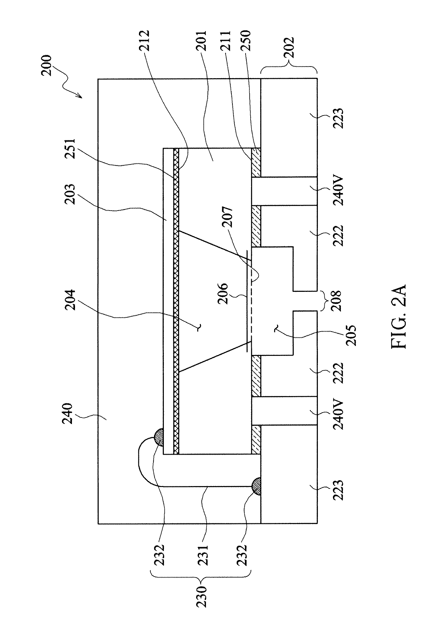
[0026]FIG. 2A shows a cross-sectional view of a MEMS package 200 according to an embodiment of the invention. The MEMS package 200 includes a MEMS chip 201, a leadframe 202, and a conductive layer 203. In the embodiment, the MEMS chip 201 is a silicon based chip having a Micro-Electro-Mechanical Systems (MEMS) device. As shown in FIG. 2A, the MEMS chip 201 has a first surface 211 and a second surface 212. The first surface 211 of the MEMS chip 201 is electrically connected to a leadframe 202. A conductive layer 203 is provided on the second surface 212 of the MEMS chip 201, which substantially covers the second surface 212. Alternatively, the conductive layer 203 covers only a part of the second surface 212. Additionally, the MEMS package 200 further includes a grounding device 230. The grounding device 230 ...


PUM


Abstract

The invention provides a MEMS package including: a MEMS chip including a first surface, a second surface, a first cavity, and a sensing device, the sensing device defining a first end of the first cavity; a leadframe including a second cavity and being electrically connected to the first surface of the MEMS chip, the second cavity being adjacent to the sensing device of the MEMS chip; a conductive layer disposed on the second surface of the MEMS chip to define a second end of the first cavity and grounded via the leadframe that is electrically connected to the conductive layer so as to provide electromagnetic shielding to the MEMS chip; and an encapsulant covering the MEMS chip, the leadframe, and the conductive layer to define an shape of the MEMS package and allowing outer surfaces of the leadframe to emerge from the MEMS package.

Description

CLAIM OF PRIORITY[0001]This application claims priority to Taiwanese Application 97142652, which was filed on Nov. 5, 2008, and which is incorporated herein by reference.BACKGROUND OF THE INVENTION[0002]1. Field of the Invention[0003]The invention relates to a MEMS package, particularly to a cavity based MEMS sensor package.[0004]2. Description of Related Art[0005]A MEMS package or a cavity based MEMS sensor package contains a MEMS chip or a cavity based MEMS sensor chip in the packaging system similar to that of integrated chips or microelectronics. FIG. 1A is a schematic cross-sectional view of a conventional MEMS chip 100 having a sensing device 110 and a resonant chamber 120. The sensing device 110, for example, can include a vibration diaphragm 111, a fixed plate 112, and a piezoresistor 113. The basic operation of the MEMS chip 100 is that when an external signal transmits via the through-holes of the fixed plate 112 to reach the vibration diaphragm 111, the signal is amplifie...

Claims


Application Information

Patent Timeline
Patent Type & Authority Applications(United States)
IPC IPC(8): H01L29/84H01L23/552H01L23/495
CPCB81B7/0064B81B2207/012H01L29/84H01L2224/48091H01L2224/48464H01L2224/73265H01L2924/00014H01L2924/3025H01L2924/00H01L2924/1461H01L2924/181H01L2924/00012
Inventor TSAO, HUNG-CHANG
Owner WINDTOP TECH CORP
Why Eureka
Try Eureka