Systems and methods for stochastic models of mask process variability

a technology of stochastic models and masks, applied in the field of simulation and error modeling of such manufacturing processes, can solve problems such as the model used in the model may not account for all mask errors or other errors introduced

Active Publication Date: 2012-11-01
MICRON TECH INC
View PDF1 Cites 14 Cited by
  • Summary
  • Abstract
  • Description
  • Claims
  • Application Information

AI Technical Summary

Problems solved by technology

However, such simulations and the models used therein may not account for all of

Method used


Image

  • Systems and methods for stochastic models of mask process variability
  • Systems and methods for stochastic models of mask process variability
  • Systems and methods for stochastic models of mask process variability

Examples


Embodiment Construction

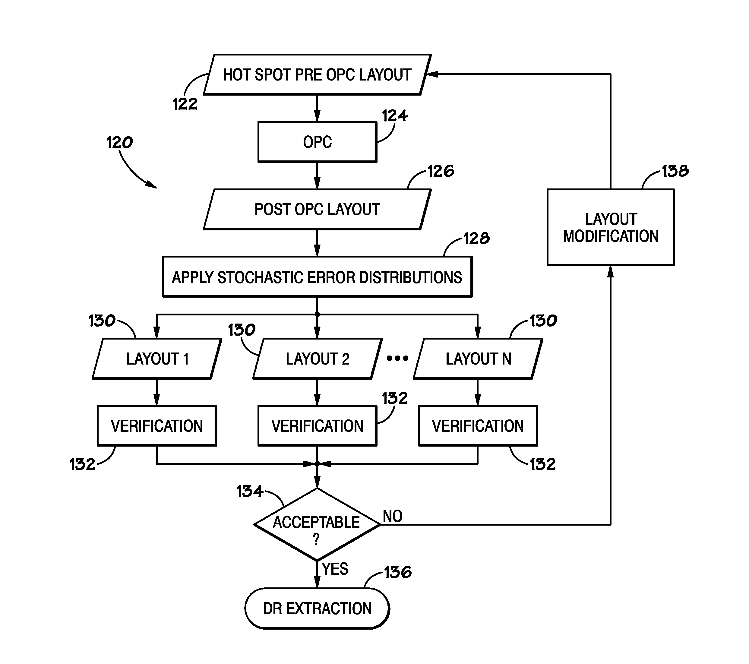
[0015]As discussed in further detail below, embodiments of the present invention include stochastic modeling of variable mask process errors of a photolithography process. In some embodiments, a simulation of a photolithography process may include application of stochastic error models generated from a probability distribution, such as a probability distribution of mask process errors. The stochastic error models may produce a plurality of mask layouts for use in analysis and configuration of the photolithography process. In some embodiments, the stochastic error modeling may be applied to critical dimension uniformity (CDU) optimization or design rule (DR) sophistication.

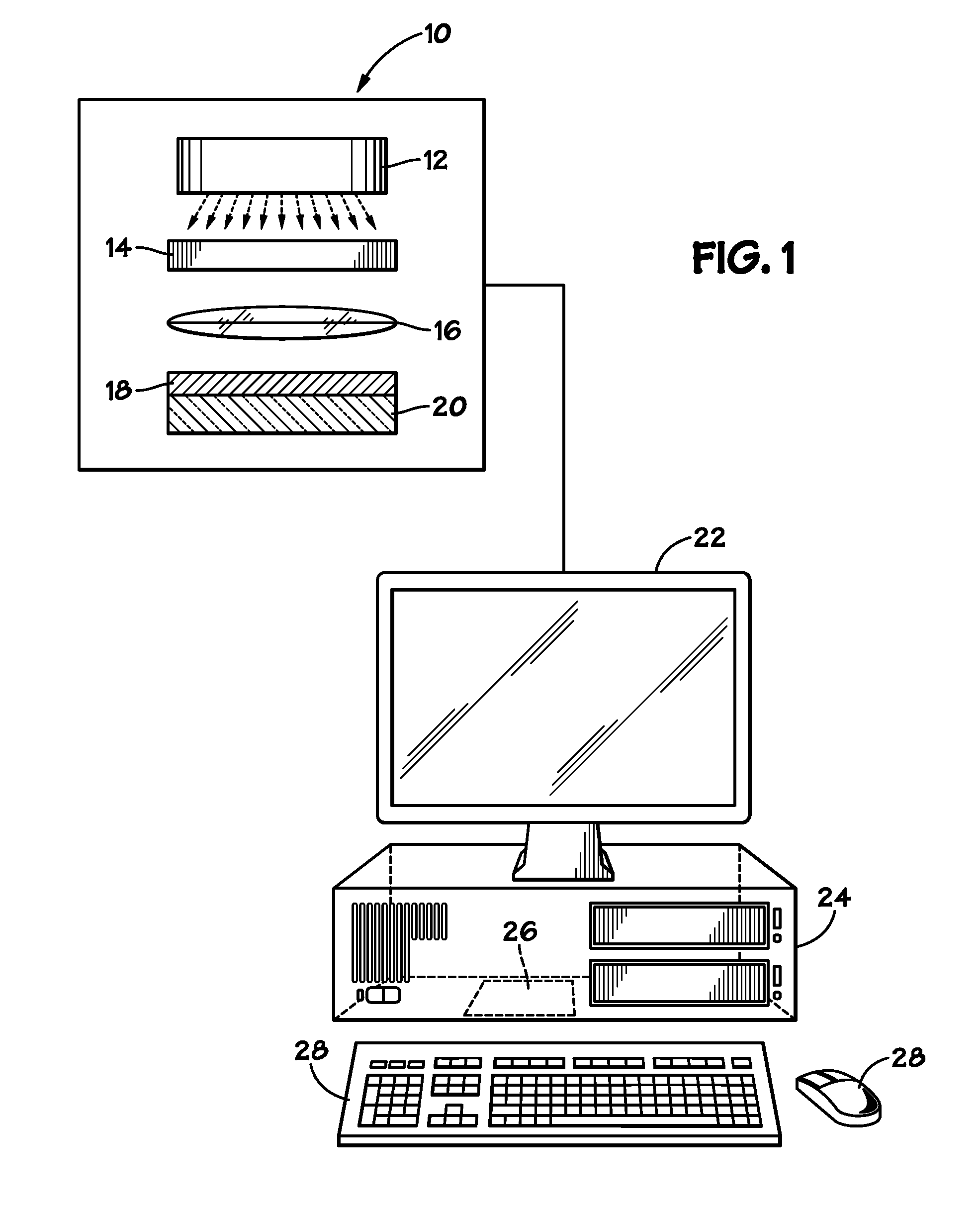
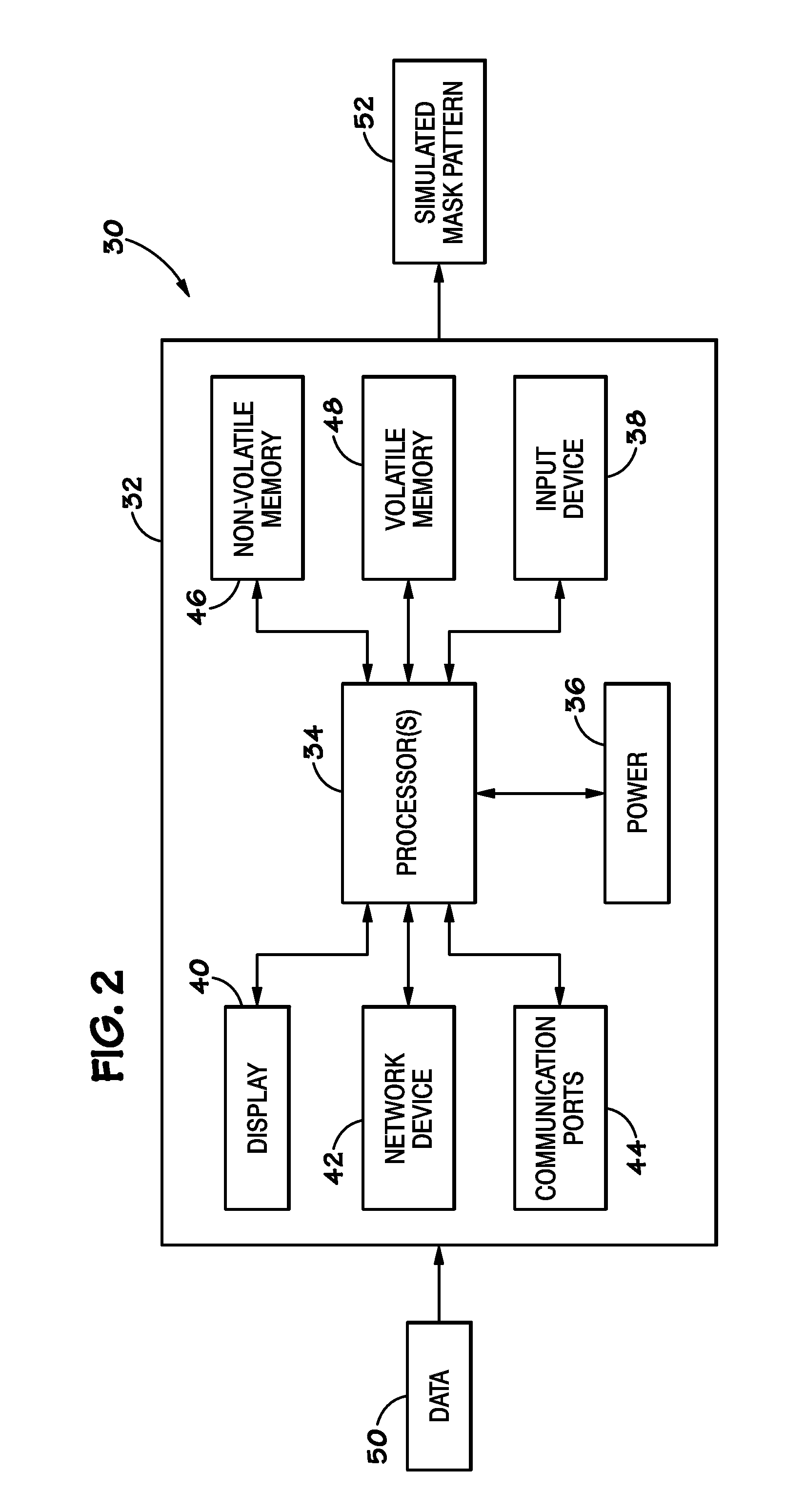
[0016]With the foregoing in mind, FIG. 1 is a simplified diagram of a photolithography system 10 in accordance with an embodiment of the present invention. The system 10 includes an illumination source 12 for producing light, a reticle 14, and a lens 16. The photolithography system 10 may use the illumination sourc...


PUM


Abstract

Systems and methods are disclosed for a stochastic model of mask process variability of a photolithography process, such as for semiconductor manufacturing. In one embodiment, a stochastic error model may be based on a probability distribution of mask process error. The stochastic error model may generate a plurality of mask layouts having stochastic errors, such as random and non-uniform variations of contacts. In other embodiments, the stochastic model may be applied to critical dimension uniformity (CDU) optimization or design rule (DR) sophistication.

Description

BACKGROUND[0001]1. Field of Invention[0002]Embodiments of the invention relate generally to semiconductor manufacturing and, more specifically, in certain embodiments, to the simulation and error modeling of such manufacturing processes.[0003]2. Description of Related Art[0004]Electronic devices are generally employed in numerous configurations to provide a variety of functions. Processing speeds, system flexibility, and size constraints are typically considered by design engineers tasked with developing electronic devices such as computer systems and system components. Such electronic devices generally include memory devices which may be used to store programs and data and which may be accessible to other system components such as processors or peripheral devices. Such memory devices may include volatile and non-volatile memory devices.[0005]The manufacture (also referred to as “fabrication”) of semiconductor devices, such as the above-described memory devices, may involve a number...

Claims


Application Information

Patent Timeline
IPC IPC(8): G06F17/50
CPCG03F7/70125G03F7/70441G06F17/50G03F1/36G03F1/68G03F7/705G06F30/00
Inventor YANG, MING-CHUANWOO, JUNG H.
Owner MICRON TECH INC
Why Eureka
Try Eureka