Method and device for nanoimprint lithography

a technology of imprinting and nano-micrometers, applied in the field of apparatus and imprinting method of nano-micrometer structure, can solve the problems of insufficient publication of the problem of limiting the risk of stamp breakage, the inability of the flexible stamp to conform to non-, and the stamp may break, so as to improve the capability of the imprinting device and reduce the deformation of the stamp

Inactive Publication Date: 2012-11-22
DANMARKS TEKNISKE UNIV +1
View PDF2 Cites 9 Cited by
  • Summary
  • Abstract
  • Description
  • Claims
  • Application Information

AI Technical Summary

Benefits of technology

[0044]By replacing the force provider with a first expandable cavity so that first and second expandable cavities are available improved uncoupled and individual control of the support pressure and the imprint pressure may be achieved since the expansion of both cavities is controllable.
[0045]Thus, use of first and second expandable cavities may improve the capability

Problems solved by technology

Accordingly, it is a problem that the stamp may break if the deformations becomes to large.
The stamp may be made more robust by making it less flexible, however at the cost of the capability of the flexible stamp to conform to non-flat imprinting surfaces.
Whereas R. H. Pedersen, et al. discloses an altern

Method used


Image

  • Method and device for nanoimprint lithography
  • Method and device for nanoimprint lithography
  • Method and device for nanoimprint lithography

Examples


Embodiment Construction

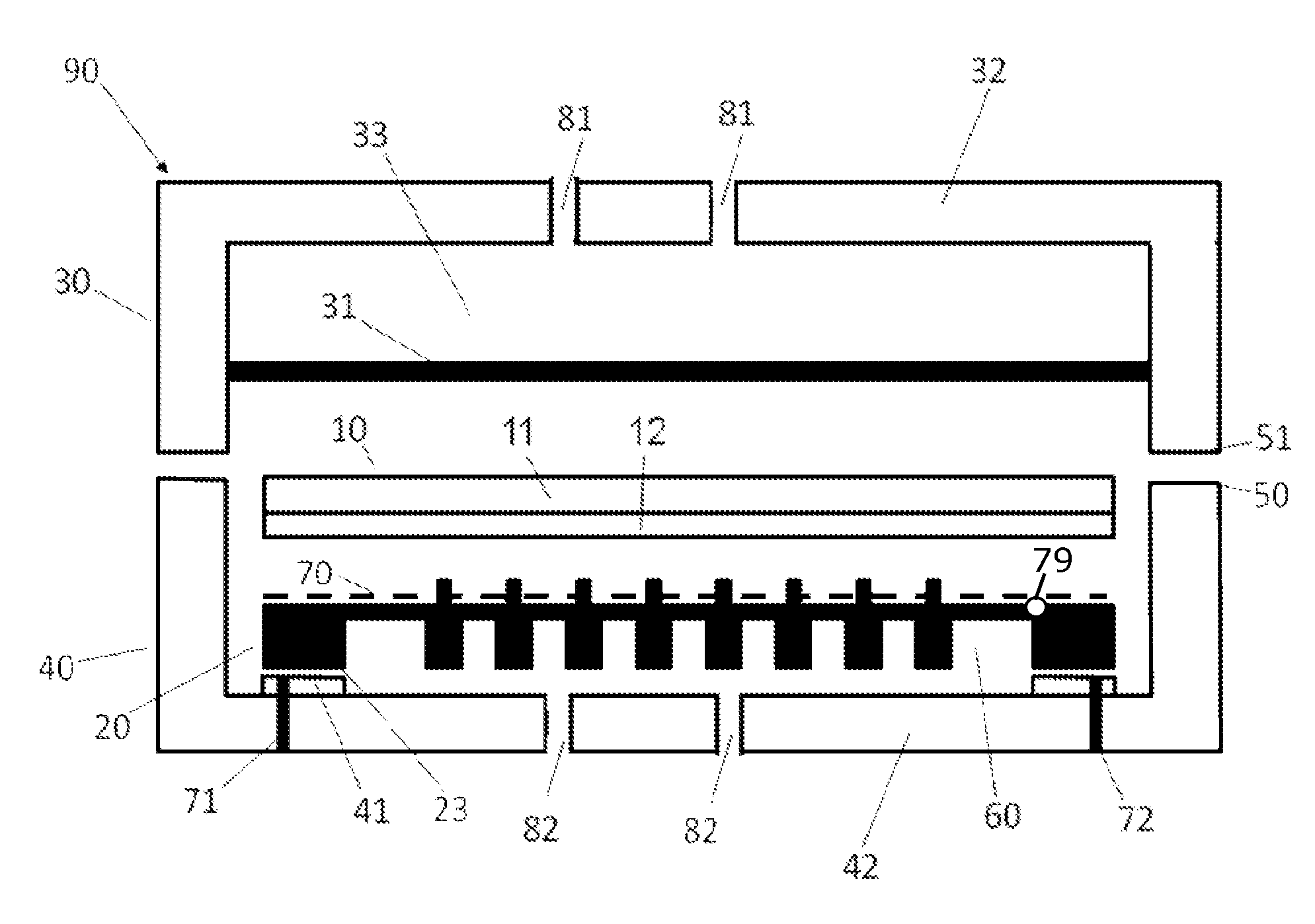
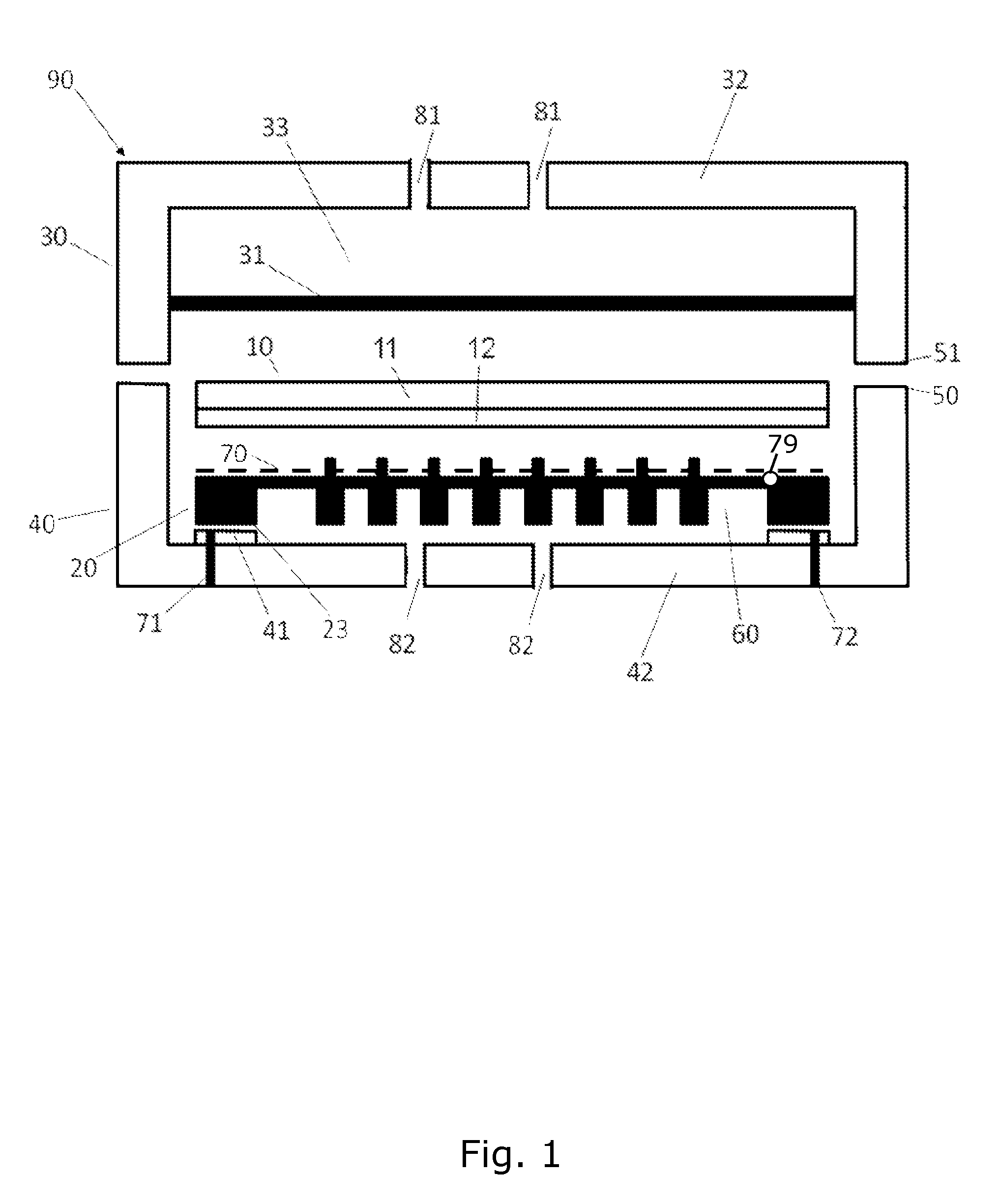
[0108]FIG. 1 illustrates an imprinting device 90 for imprinting nano or micro features in or on an associated substrate 10 by means of an associated stamp 20. Said substrate may comprise an imprintable material 12, such as an imprint resist 12, provided on a back 11, such as a silicon, glass or metal plate.

[0109]In the context of the present invention, it is to be understood that imprinting nano or micro meter features may relate to imprinting features having dimensions being less than 100 micrometers, preferably less than 50 micrometers, or more preferably less than 25 micrometers.

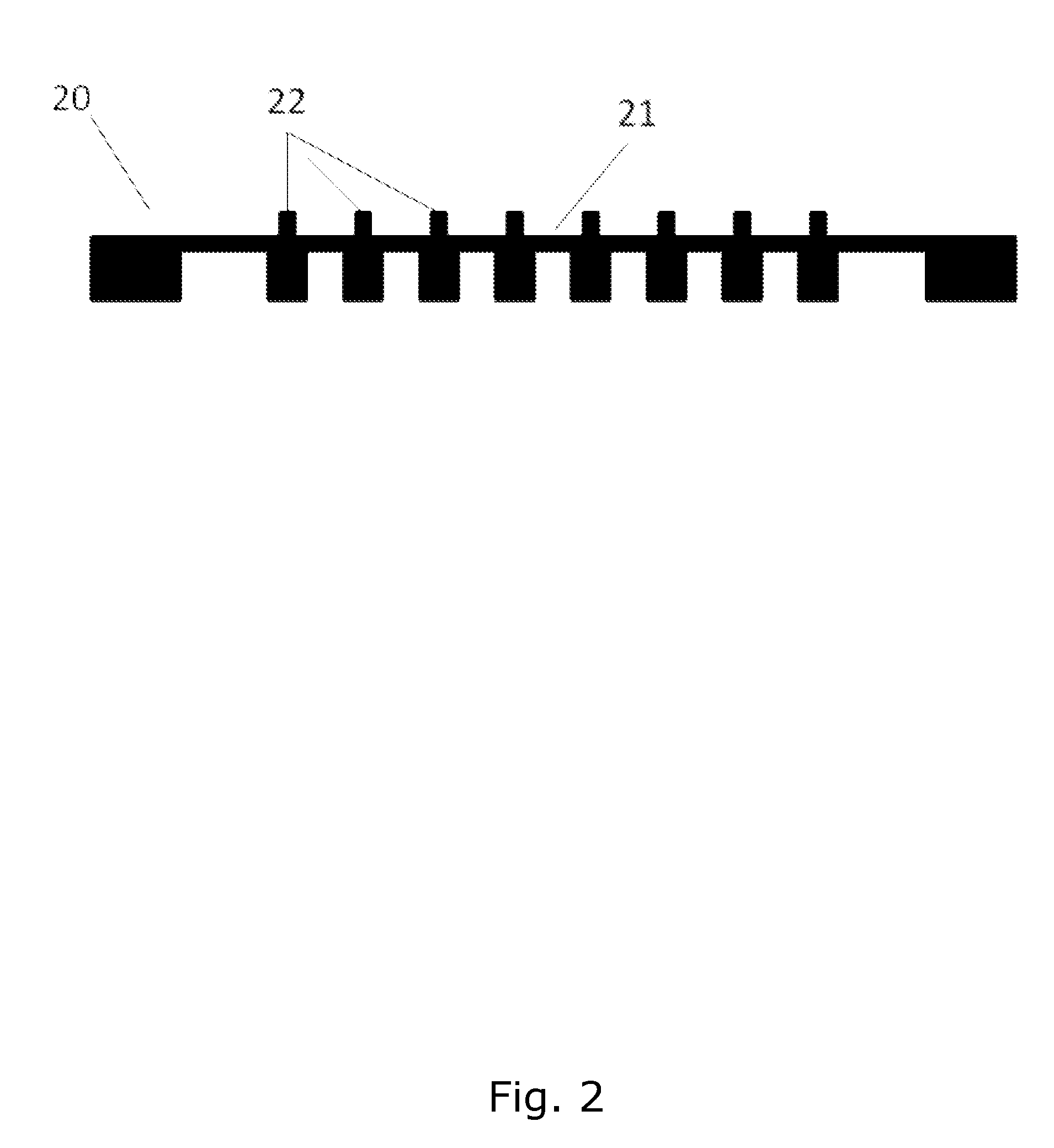
[0110]In an embodiment shown in FIG. 2, the above-mentioned stamp may comprise an elastically bendable base part 21, possibly having a flexible membrane-like structure and imprinting features 22 protruding from the base part 21. The stamp 20 may be monolithically formed from a single piece of material. For example, the stamp may be produced from a silicon wafer and the imprinting features 22 may made by o...


PUM

PropertyMeasurementUnit
Pressureaaaaaaaaaa
Flexibilityaaaaaaaaaa
Heightaaaaaaaaaa

Abstract

The invention relates to an imprinting device for imprinting nano/micro structures. The imprinting device comprises a second expandable cavity constituted in part by a membrane of the stamp. The membrane is flexible and formed in such a way so that when fluid is pumped into the expandable cavity then the membrane expands towards the imprintable substrate and imprints the substrate. The imprinting device is further provided with a force provider, alternatively a first expandable cavity, for forcing a contact part of the substrate to make contact with a matching contact part of the stamp.

Description

FIELD OF THE INVENTION[0001]The invention relates to an apparatus and a method for imprinting of nano and micrometer structures, and particularly to such apparatus and method being based on a flexible stamp.BACKGROUND OF THE INVENTION[0002]Nano imprint lithography (NIL) is a method for producing nano- and micrometer structures in imprintable materials by forcing a stamp with imprinting structures into an imprintable material. The imprinting structures are formed on a face of the stamp and the stamp itself may be rigid or flexible.[0003]In cases where the stamp is flexible, the stamp deforms when it is pressed against the imprintable structure. Accordingly, it is a problem that the stamp may break if the deformations becomes to large. The stamp may be made more robust by making it less flexible, however at the cost of the capability of the flexible stamp to conform to non-flat imprinting surfaces. Thus, it is desirable to have a stamp which is flexible but also robust.[0004]R. H. Ped...

Claims


Application Information

Patent Timeline
IPC IPC(8): B29C59/02B82Y30/00
CPCB82Y10/00B82Y40/00G03F9/7053G03F9/7042G03F7/0002
Inventor SMISTRUP, KRISTIANHEDEGAARD, TOBIASHANSEN, OLE
Owner DANMARKS TEKNISKE UNIV
Why Eureka
Try Eureka