Electronic component and method of manufacturing electronic component

a technology of electronic components and manufacturing methods, applied in the field of surface mounting electronic components, can solve the problems of short circuit between the electrodes of the electronic components, difficult to achieve close adjacent high-density mounting in which the distance between the electronic components b>101/b> is small, and the likelihood of short circui

Active Publication Date: 2012-12-13
TDK CORPARATION
View PDF5 Cites 28 Cited by
  • Summary
  • Abstract
  • Description
  • Claims
  • Application Information

AI Technical Summary

Benefits of technology

[0013]The present invention can manufacture electronic components enabling high-density mounting, in which no solder fillets are formed in portions on the side face sides in the electronic components at the time of mounting, so that no short-circuiting is caused by solder bridges and the like between the electronic components adjacent to each other even when close adjacency mounting is performed as mentioned above.

Problems solved by technology

Therefore, a problem of short-circuiting is more likely to occur between the electronic components 101, thus making it harder to achieve close adjacent high-density mounting in which the distance between the electronic components 101 is small.
This may cause short-circuiting between the electrodes of the electronic components 101.

Method used


Image

  • Electronic component and method of manufacturing electronic component
  • Electronic component and method of manufacturing electronic component
  • Electronic component and method of manufacturing electronic component

Examples


Embodiment Construction

[0038]In the following, preferred embodiments of the present invention will be explained in detail with reference to the accompanying drawings. In the explanation, the same constituents or those having the same functions will be referred to with the same signs while omitting their overlapping descriptions.

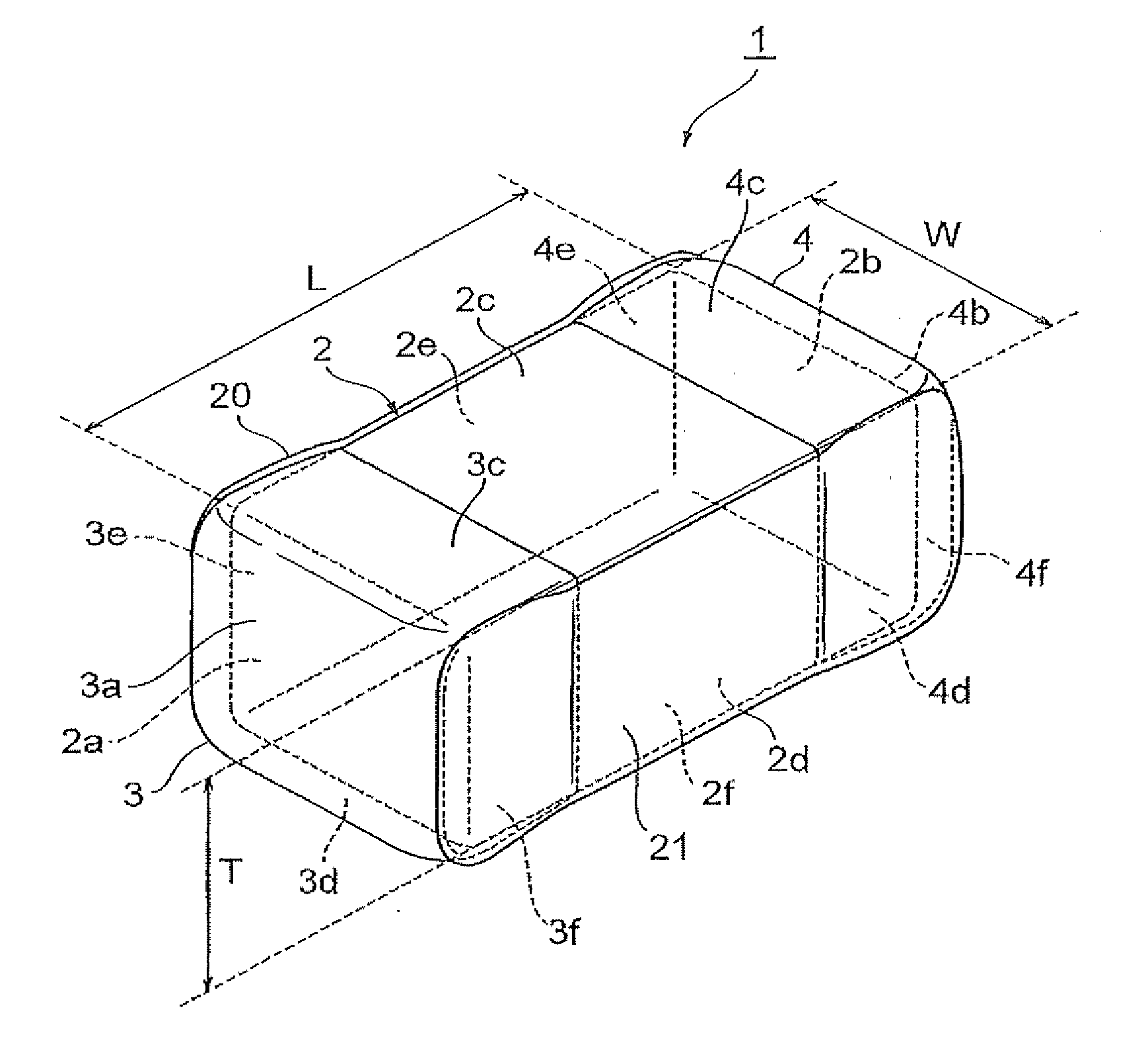
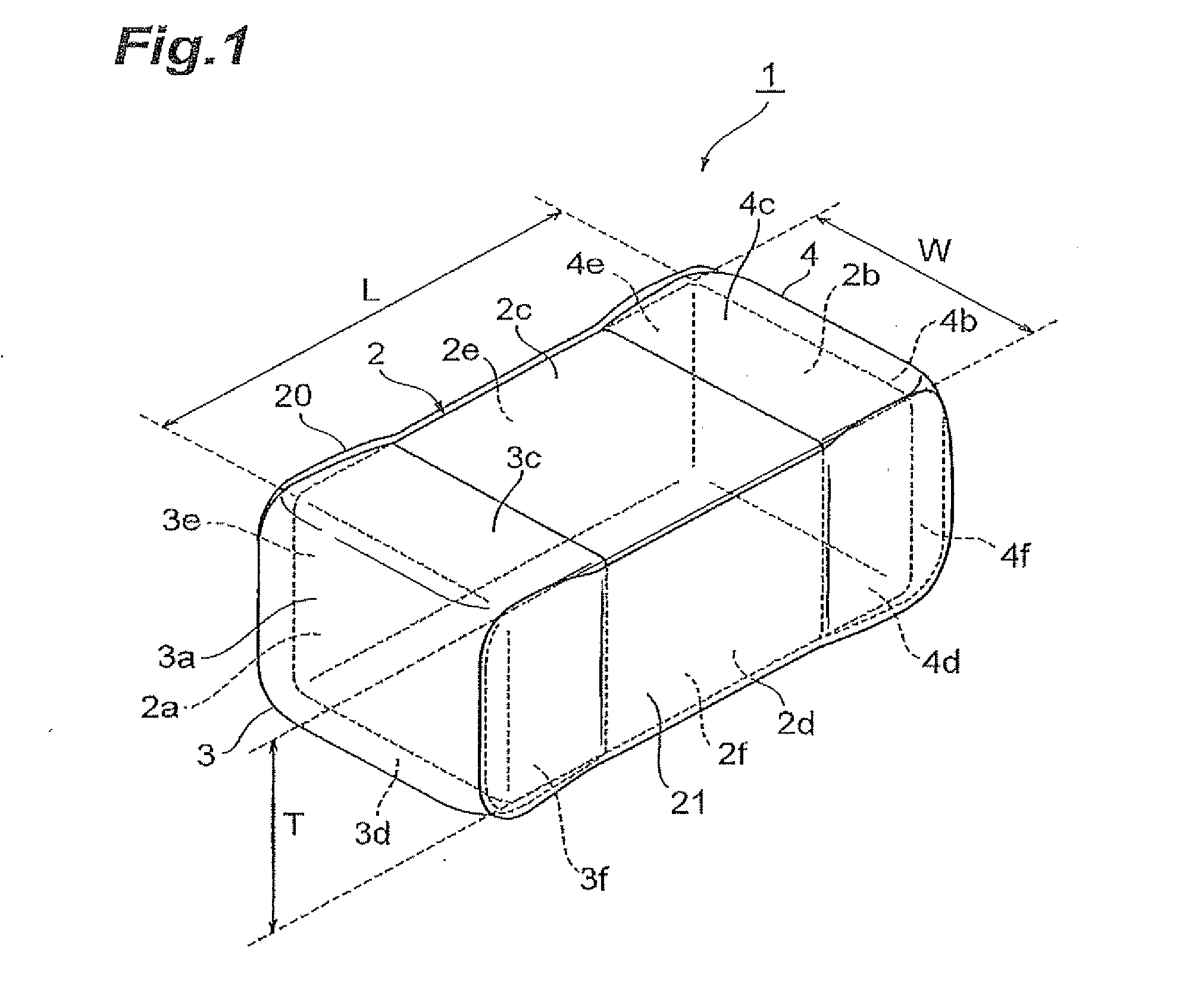
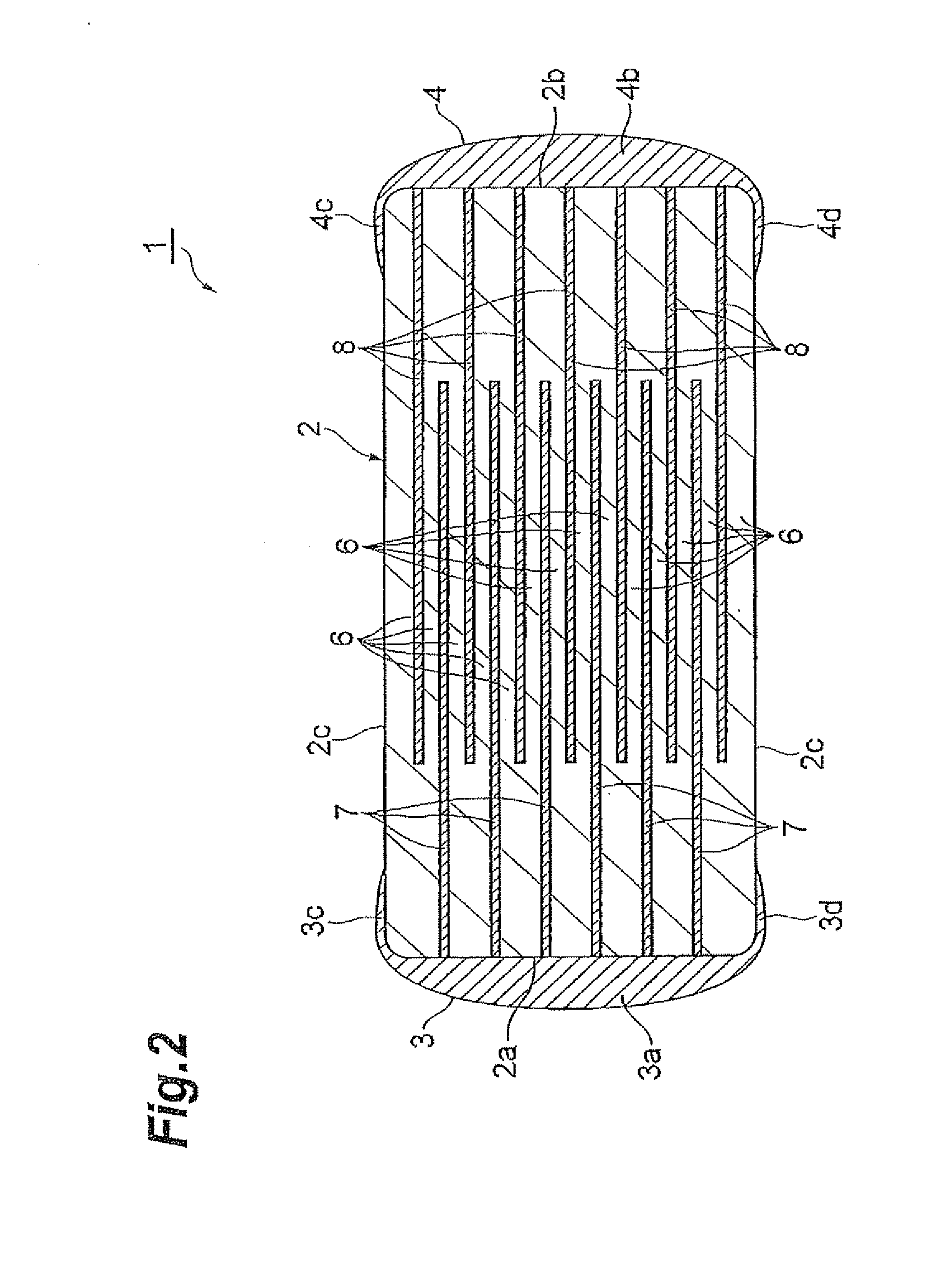
[0039]With reference to FIGS. 1 and 2, structures of an electronic component 1 in accordance with an embodiment will be explained. FIG. 1 is a perspective view illustrating the electronic component in accordance with this embodiment, FIGS. 2 and 3 are diagrams for explaining cross-sectional structures of the electronic component in accordance with the embodiment. FIG. 3 does not depict inner electrodes 7, 8 which will be explained later and the like.

[0040]The electronic component 1 is an electronic component such as a multilayer ceramic capacitor, for example. The electronic component 1 comprises an element body 2 and outer electrodes 3, 4. The element body 2 is constructed as a re...


PUM

PropertyMeasurementUnit
thicknessaaaaaaaaaa
temperatureaaaaaaaaaa

Abstract

An electronic component comprises an element body and an outer electrode. The element body has a pair of end faces opposing each other, a pair of main faces opposing each other while extending so as to connect the pair of end faces to each other, and a pair of side faces opposing each other while extending so as to connect the pair of main faces to each other. The outer electrode is formed on the end face side of the element body and covers a portion of the main and side faces adjacent to the end face. At least a surface of an electrode portion of the outer electrode located on the side face side thereof is covered with an insulating layer.

Description

BACKGROUND OF THE INVENTION[0001]1. Field of the Invention[0002]The present invention relates to an electronic component, a surface mounting type electronic component in particular, and a method of manufacturing the same.[0003]2. Related Background Art[0004]Conventionally, as a method of manufacturing a surface mounting type electronic component (e.g., a multilayer ceramic capacitor), the following method has been used widely (see, for example, Japanese Patent Application Laid-Open No. 2006-13315). Green sheets and inner electrode materials are alternately stacked and then fired, so as to form an element body. End faces of the element body are dipped into a conductive paste, and the conductive paste applied to the element body is dried, so as to form paste layers on the element body. Thereafter, the paste layers are sintered and then plated for improving soldability, so as to form outer electrodes on the element body.SUMMARY OF THE INVENTION[0005]In the above-mentioned conventional ...

Claims


Application Information

Patent Timeline
Patent Type & Authority Applications(United States)
IPC IPC(8): B05D5/12H01L41/047H01C7/10H01G4/01H01F5/00
CPCH01G4/30H01G4/12H05K2203/046H01G4/2325H05K3/3442H01G4/232H01G4/012H01G4/248H05K1/181
Inventor SHIRAKAWA, YUKIHIKOINAGAKI, TATSUOKON, SHINTAROHIROSE, OSAMUKONNO, MASAHIKO
Owner TDK CORPARATION
Why Eureka
Try Eureka