Display device

a technology of display panel and display screen, which is applied in the field of display panel, can solve the problems of reduced resistance, defects of liquid crystal display panel, air bubbles in the display panel, etc., and achieve the effect of preventing the reduction of push resistance, reducing the allowance of bonding margin, and reducing the push resistan

Inactive Publication Date: 2012-12-13
JAPAN DISPLAY INC
View PDF10 Cites 8 Cited by
  • Summary
  • Abstract
  • Description
  • Claims
  • Application Information

AI Technical Summary

Benefits of technology

[0010]When the contact area of the columnar spacer to the TFT substrate is large, the repulsion force between the TFT substrate and the CF substrate is strong, often causing air bubbles in the liquid crystal display panel. On the other hand, when the contact area of the columnar spacer to the TFT substrate is small, the push resistance is reduced, often causing uneven brightness and liquid crystal leakage.
[0011]Thus, in the liquid crystal display panel using the ODF method, the density of main columnar spacers is reduced so that the contact area of the main columnar spacers to the TFT substrate is smaller than that of the conventional liquid crystal display panel. Then, the reduction of the push resistance is prevented by sub columnar spacers.
[0012]In this case, when displacement occurs in the bonding process of the TFT substrate and the CF substrate, the low density contact area of the main columnar spacers to the TFT substrate varies, causing uneven brightness and liquid crystal leakage due to the reduction in the push resistance. In the ODF method, the variability of the contact area of the main columnar spacers to the TFT substrate is large. As a result, the allowance of the bonding margin is reduced.
[0013]The present invention has been made to solve the above problems of the related art. An object of the present invention is to provide a technology that can reduce the variability of the area in which the top of columnar spacers contacts a first substrate bonded to a second substrate in a display device, such as a liquid crystal display device in which liquid crystal is injected between the substrates or an organic EL display device having a gap between the substrates, when displacement occurs in the bonding process of the first and second substrates.

Problems solved by technology

In the ODF method, defects often occur due to the size of the area in which the columnar spacer contacts the TFT substrate to constantly maintain the gap distance between the TFT substrate and the CF substrate.
When the contact area of the columnar spacer to the TFT substrate is large, the repulsion force between the TFT substrate and the CF substrate is strong, often causing air bubbles in the liquid crystal display panel.
On the other hand, when the contact area of the columnar spacer to the TFT substrate is small, the push resistance is reduced, often causing uneven brightness and liquid crystal leakage.
In this case, when displacement occurs in the bonding process of the TFT substrate and the CF substrate, the low density contact area of the main columnar spacers to the TFT substrate varies, causing uneven brightness and liquid crystal leakage due to the reduction in the push resistance.

Method used


Image

  • Display device
  • Display device
  • Display device

Examples


first embodiment

[0026]A liquid crystal display device according to a first embodiment includes a so-called In-Plane-Switching (IPS) liquid crystal display panel that drives liquid crystal molecules by applying an electric field between a pixel electrode and a counter electrode formed in one of a pair of glass substrates.

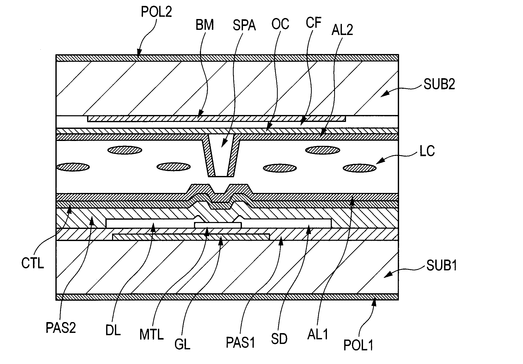
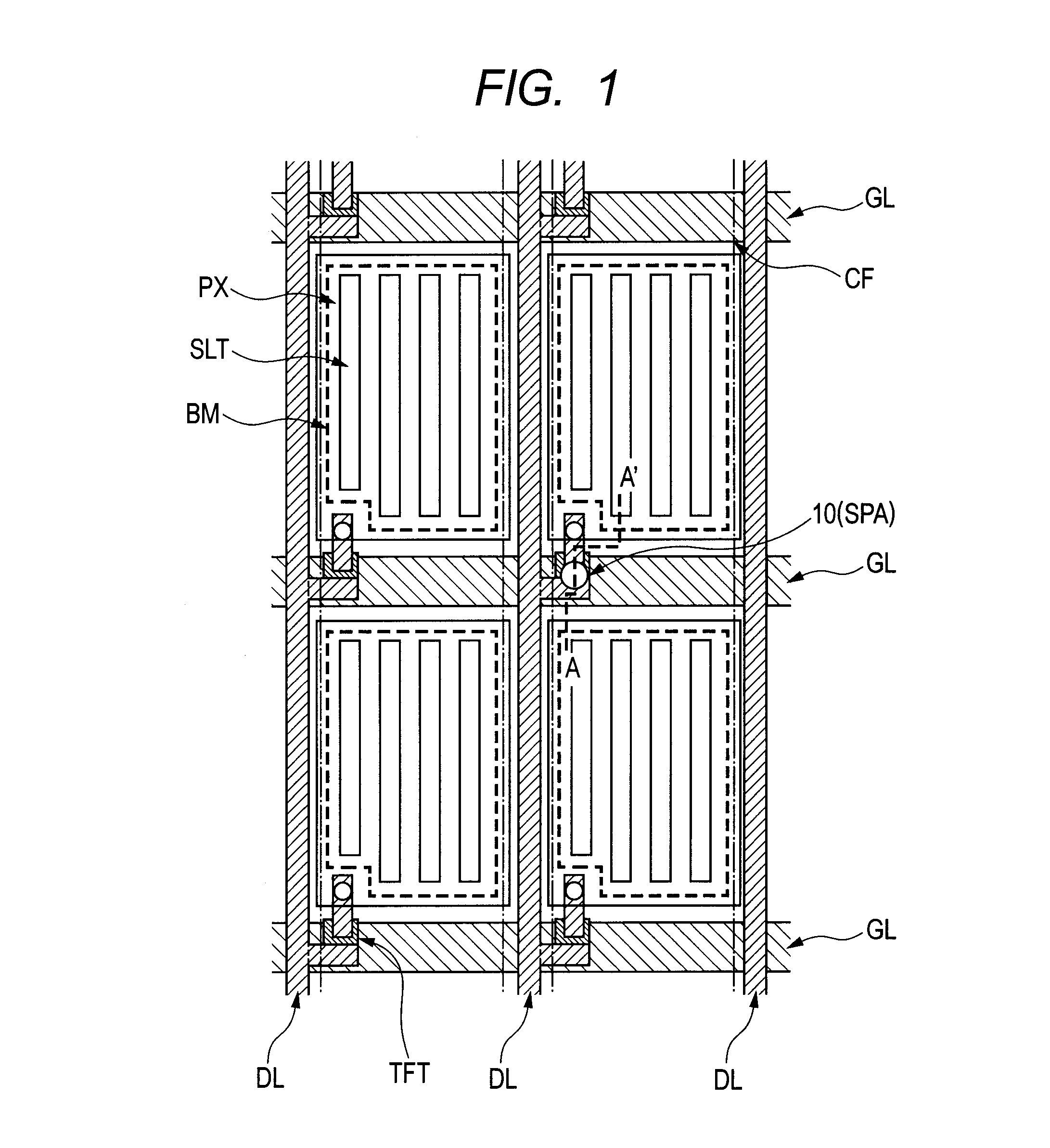
[0027]FIG. 1 is a top view of the electrode structure of a liquid crystal display panel according to an embodiment of the present invention. FIG. 2 is a cross-sectional view taken along line A-A′ of FIG. 1.

[0028]In the liquid crystal display panel according to this embodiment, a TFT substrate (a first substrate according to the present invention) and a CF substrate (a second substrate according to the present invention) are provided with a liquid crystal layer (LC) sandwiched between the two substrates.

[0029]As shown in FIG. 2, the TFT substrate has a transparent substrate (for example, a glass substrate) (SUB1). On the liquid crystal layer side of the transparent substrate (SUB1), ...


PUM

PropertyMeasurementUnit
areaaaaaaaaaaa
distanceaaaaaaaaaa
gap distanceaaaaaaaaaa

Abstract

The present invention relates to a display device such as a liquid crystal display device including a first substrate and a second substrate with liquid crystal injected between the first and second substrates. In the display device, the second substrate includes a plurality of columnar spacers, and the first substrate has a protrusion in an area facing the top of the columnar spacer. The plurality of columnar spacers formed on the second substrate are not arranged at even intervals in the longitudinal direction of the scan line, and / or are not aligned on the line but are arranged at random.

Description

CLAIM OF PRIORITY[0001]The present application claims priority from Japanese Patent Application JP2011-127837 filed on Jun. 8, 2011, the content of which is hereby incorporated by reference into this application.BACKGROUND OF THE INVENTION[0002]1. Field of the Invention[0003]The present invention relates to a display device, and more particularly, to a display device in which a columnar spacer (a cylindrical spacer, a post-like spacer or the like) is provided between a first substrate and a second substrate to keep the distance between the substrates constant.[0004]2. Description of the Related Art[0005]Examples of conventionally known display devices include a liquid crystal display device in which a liquid crystal is injected between a pair of substrates, an organic EL display device in which an organic light emitting device is formed between a pair of substrates, and a display device including a mechanical drive device such as MEMS. For example, in the production process of liqui...

Claims


Application Information

Patent Timeline
Patent Type & Authority Applications(United States)
IPC IPC(8): G02F1/1339
CPCG02F1/133371G02F2201/14G02F1/13394G02F1/13392G02F1/13415G02F1/133512G02F1/1341G02F1/136286
Inventor DOI, KOSUKEKOSHITA, TOSHIYUKI
Owner JAPAN DISPLAY INC
Why Eureka
Try Eureka