IP protection

a technology of IP protection and information, applied in the field of IP protection, can solve the problems of high production cost and risk, and achieve the effect of reducing the disclosure of ip information

Active Publication Date: 2012-12-20
RENESAS ELECTRONICS CORP +2
View PDF2 Cites 27 Cited by
  • Summary
  • Abstract
  • Description
  • Claims
  • Application Information

AI Technical Summary

Benefits of technology

[0004]A method of forming a device is disclosed. The method includes providing a MPW mask having a plurality of chiplets pertaining to a plurality of IP owners. Non-relevant chiplet or chiplets of an IP owner are implemented with IP protection. A substrate is patterned using th

Problems solved by technology

As the size of the device becomes smaller, this however leads to higher production cost.
Nevertheless, there could be risk

Method used


Image

  • IP protection
  • IP protection
  • IP protection

Examples


Embodiment Construction

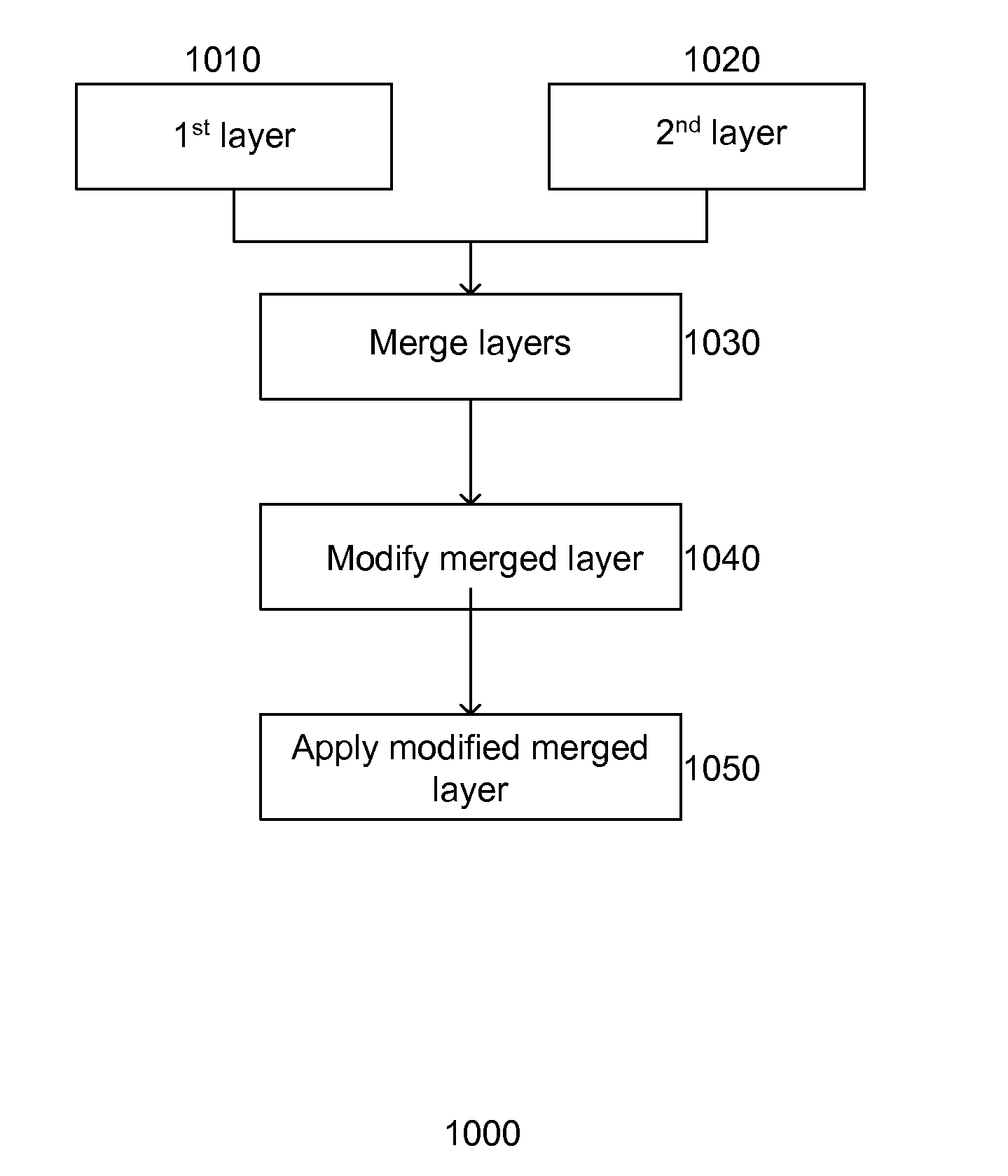
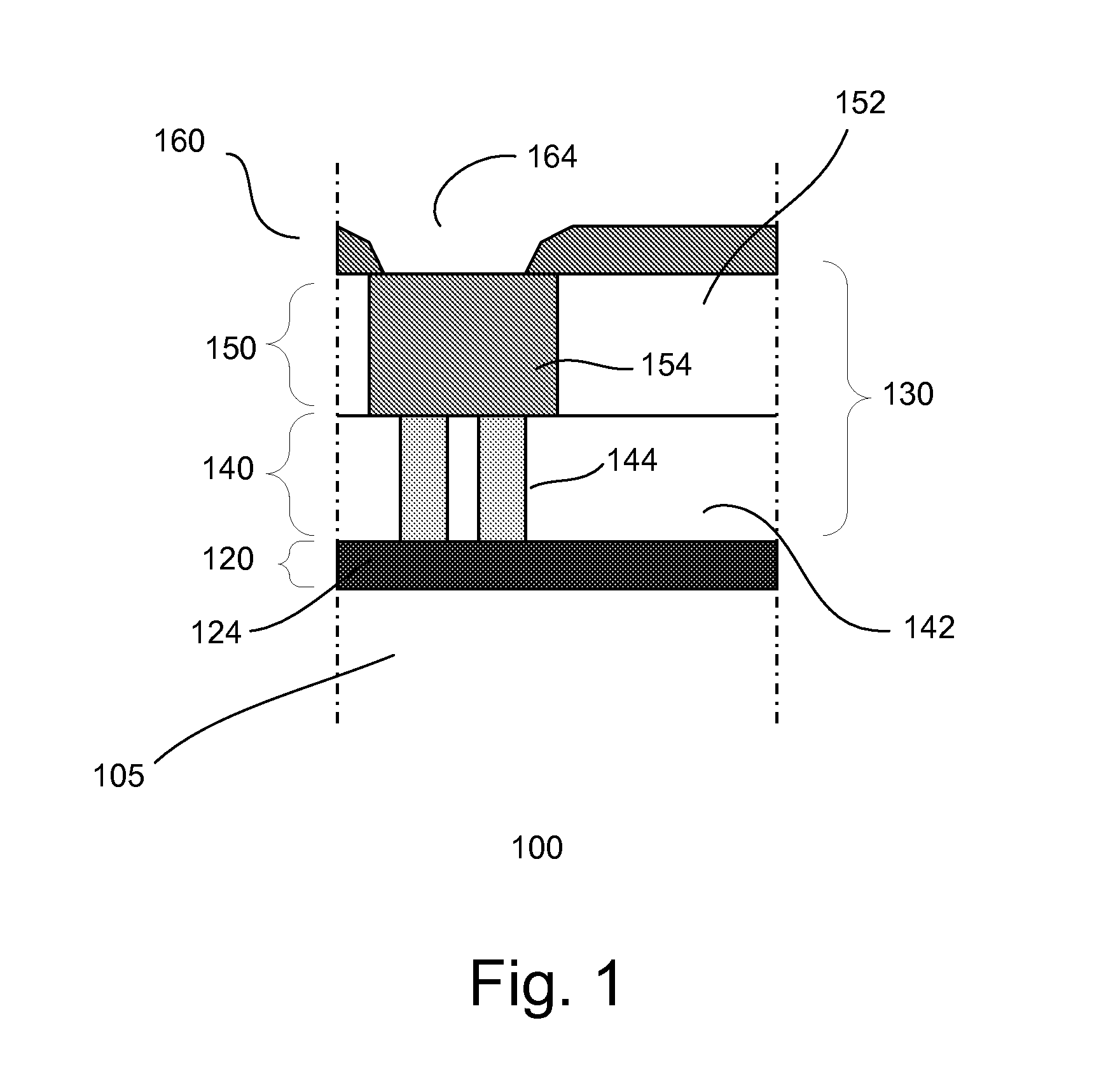
[0021]The fabrication of devices, such as integrated circuits (ICs), involves the formation of features on a substrate that make up circuit components, such as transistors, resistors and capacitors. The devices are interconnected, enabling the device to perform the desired functions. Interconnections are formed by forming contacts and conductive lines in a dielectric layer using, for example, damascene techniques. The features and interconnections are formed by repeatedly depositing and patterning layers on the wafer. The devices may have multiple interconnection layers. The structures of the different layers of the device are created or patterned using respective mask and etch techniques.

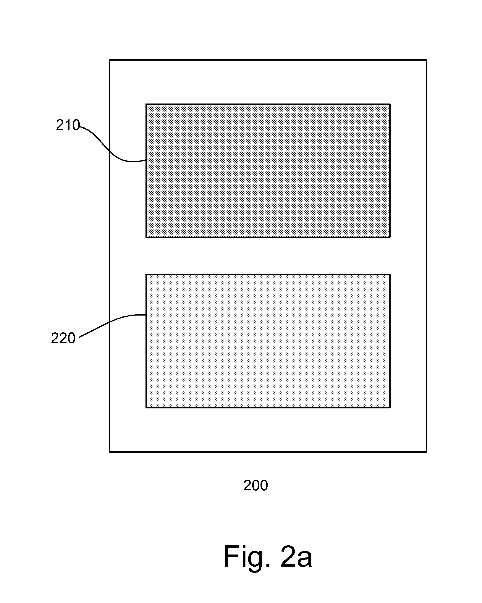
[0022]The various features and interconnections are strategically placed on the device to minimize the use of space and / or optimize performance. The placement of various features and interconnections is referred to as a product or device layout. The layers which form the components are in the lower...


PUM


Abstract

Multi-Project Wafers includes a plurality of chiplets from different IP owners. Non-relevant chiplets are implemented with IP protection to inhibit IP disclosure of non-relevant IP owners.

Description

BACKGROUND[0001]Miniaturization of portable consumer products such as MP3 players, mobile phones, and digital camera is driving the need for smaller devices such as integrated circuits (IC) with high memory density and more functionality. As the size of the device becomes smaller, this however leads to higher production cost.[0002]To reduce the fabrication cost, Multi-Projects-Wafer (MPW) is proposed as it offers the solution to integrate onto wafers a number of different designs modules which may also include intellectual property (IP) resources from various vendors or parties. Nevertheless, there could be risks where intellectual property (IP) resources from the various parties are exposed to third parties including competitors.[0003]From the foregoing discussion, it is desirable to produce devices with low production cost and sufficient IP protection. It is also desirable to ensure IP protection during the delivery of the devices.SUMMARY OF THE INVENTION[0004]A method of forming ...

Claims


Application Information

Patent Timeline
IPC IPC(8): H01L29/06G06F17/50
CPCG06F2217/66G06F17/5068H01L27/0207H01L22/32
Inventor TAN, SOON YOENGTANG, TECK JUNGMELVILLE, IAN D.YAO, YELEI VIANNAYAMAGATA, YASUSHI
Owner RENESAS ELECTRONICS CORP
Why Eureka
Try Eureka