Light-Emitting Device, Electronic Device, and Lighting Device

a technology of light-emitting devices and electronic devices, which is applied in the direction of semiconductor devices, diodes, electrical devices, etc., can solve the problems of difficult lighting devices to display bright colors or desired colors, and achieve the effect of reducing power consumption of light-emitting devices and less uneven luminan

Inactive Publication Date: 2013-01-03
SEMICON ENERGY LAB CO LTD
View PDF4 Cites 43 Cited by
  • Summary
  • Abstract
  • Description
  • Claims
  • Application Information

AI Technical Summary

Benefits of technology

[0009]In order to put displays and lighting devices using organic EL elements into practical use, it has been required to reduce power consumption of light-emitting devices using organic EL elements. In addition, high-quality light-emitting devices which can emit light of a bright color and have less luminance unevenness have been required.

Problems solved by technology

In particular, occurrence of unintentional light emission of a light-emitting element in adjacent light-emitting units emitting light of different colors makes it difficult for the light-emitting device to display a desired color or a bright color.

Method used


Image

  • Light-Emitting Device, Electronic Device, and Lighting Device
  • Light-Emitting Device, Electronic Device, and Lighting Device
  • Light-Emitting Device, Electronic Device, and Lighting Device

Examples


embodiment 1

[0052]In this embodiment, a light-emitting device according to one embodiment of the present invention is described with reference to FIGS. 1A to 1D, FIGS. 2A to 2D, and FIGS. 3A to 3D.

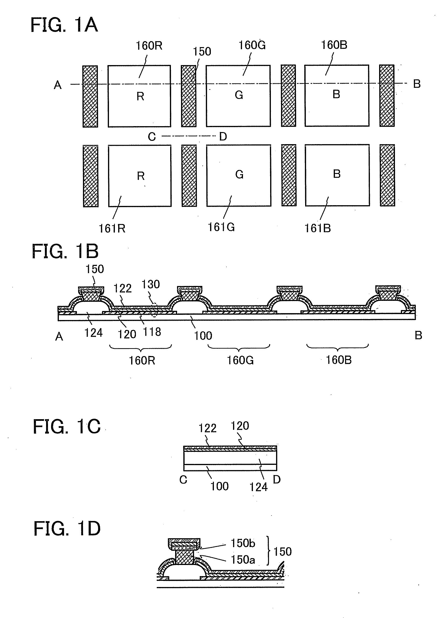
[0053]The light-emitting device according to one embodiment of the present invention includes a plurality of light-emitting units. Each light-emitting unit includes a light-emitting element which includes a layer (EL layer) containing an organic compound between a first electrode and a second electrode. The first electrode is separated between light-emitting elements. The EL layer includes a layer containing a light-emitting substance and a layer having high conductivity provided between the first electrode and the layer containing a light-emitting substance. Accordingly, a light-emitting element having low driving voltage or a light-emitting device with low power consumption can be achieved in one embodiment of the present invention.

[0054]In addition, the light-emitting device according to one embodi...

embodiment 2

[0088]In this embodiment, a light-emitting device according to one embodiment of the present invention is described with reference to FIGS. 4A to 4C. The light-emitting device according to one embodiment of the present invention, which includes a common wiring outside a light-emitting portion including the light-emitting units described in Embodiment 1, is described in detail.

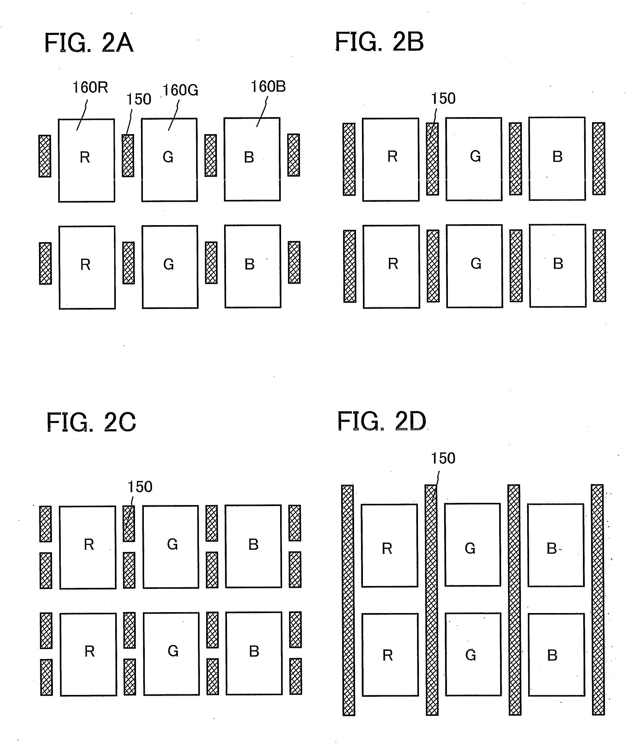
[0089]In the light-emitting device according to one embodiment of the present invention, light-emitting units emitting light of the same color arranged in one direction include a second electrode formed from one layer. The common wiring is electrically connected to the second electrode and supplies a common potential to the second electrode. This structure can suppress a potential drop of the second electrode, thereby providing a high-quality light-emitting device with less luminance unevenness.

[0090]FIGS. 4A to 4C illustrate examples of the positional relation between the inversely tapered partitions 150, the ...

embodiment 3

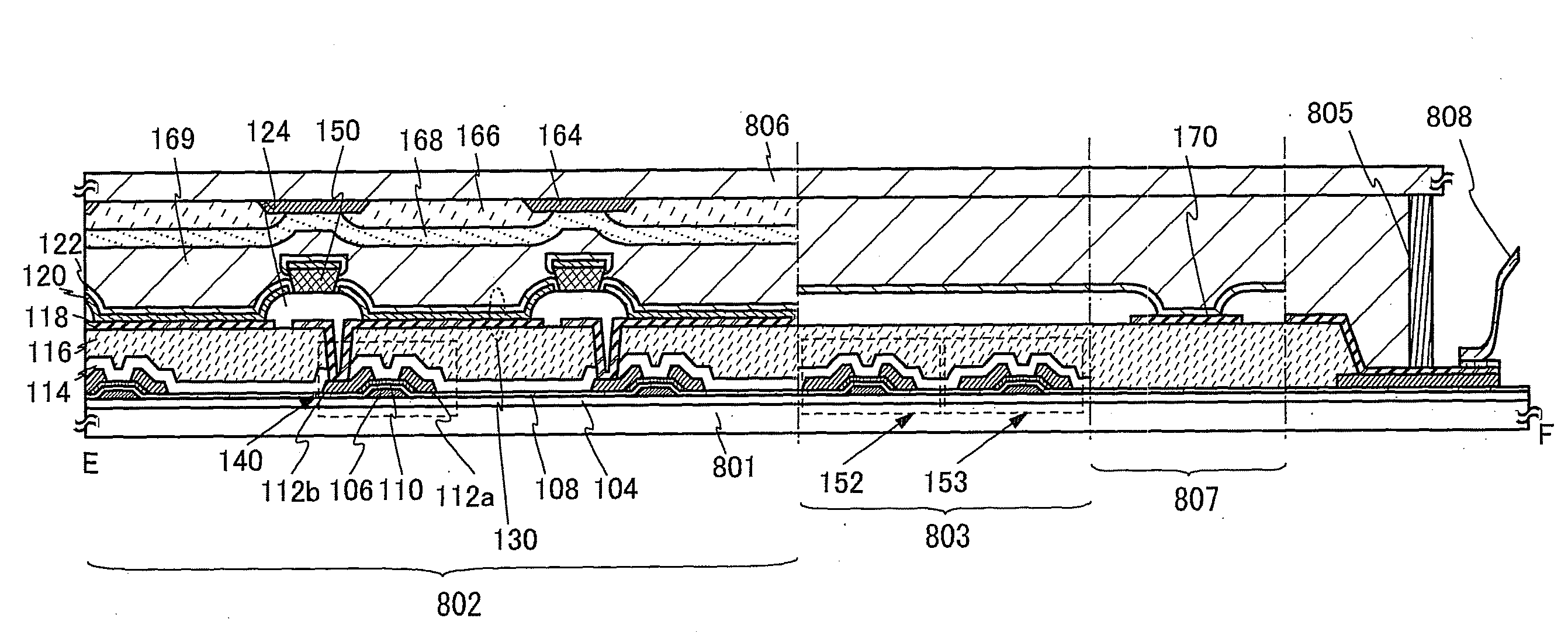
[0100]A light-emitting device according to one embodiment of the present invention is described with reference to FIGS. 5A and 5B and FIG. 9. FIG. 9 is a plan view of a light-emitting device and FIGS. 5A and 5B are cross-sectional views taken along chain line E-F in FIG. 9. In FIG. 9, some of the components, e.g., an insulating layer 104, are omitted. The structures in FIGS. 5A and 5B are the same except for the structure of the partition.

[0101]A light-emitting device in this embodiment includes a plurality of light-emitting units in a light-emitting portion. Each light-emitting unit includes a light-emitting element which includes an EL layer between a first electrode and a second electrode. The first electrode is separated between light-emitting elements. The EL layer includes a layer containing a light-emitting substance and a layer having high conductivity provided between the first electrode and the layer containing a light-emitting substance. Accordingly, a light-emitting devi...


PUM


Abstract

A high-quality light-emitting device having low power consumption, capability of emitting light of a bright color, and less luminance unevenness is provided. Provided is a light-emitting device in which a plurality of light-emitting units each include a light-emitting element which includes a layer (EL layer) containing an organic compound between a first electrode and a second electrode. The first electrode is separated between light-emitting elements. The EL layer includes a layer (light-emitting layer) containing a light-emitting substance and a layer containing a donor substance and an acceptor substance provided between the first electrode and the light-emitting layer. An inversely tapered partition is provided only between adjacent light-emitting units emitting light of different colors.

Description

BACKGROUND OF THE INVENTION[0001]1. Field of the Invention[0002]The present invention relates to a light-emitting device, an electronic device, and a lighting device utilizing organic electroluminescence (EL).[0003]2. Description of the Related Art[0004]A light-emitting element using an organic compound as a light-emitting body, which has characteristics such as feasibility of being thinner and lighter, high speed response to input signals, and capability of direct current low voltage driving, has been expected to be applied to next-generation flat panel displays or lighting devices. In particular, a display device in which light-emitting elements are arranged in a matrix is considered to have advantages of a wide viewing angle and excellent visibility over a conventional liquid crystal display device.[0005]The emission mechanism of a light-emitting element (organic EL element) using an organic compound as a light-emitting body is as follows. First, when voltage is applied between a...

Claims


Application Information

Patent Timeline
Patent Type & Authority Applications(United States)
IPC IPC(8): H01L33/36H01L33/48
CPCH01L51/006H01L51/0072H01L51/0085H01L51/506H01L51/5064H01L51/5076H01L27/3276H01L51/525H01L51/5278H01L27/3211H01L27/322H01L27/3246H01L51/508H10K59/35H10K59/38H10K59/122H10K59/131H10K85/633H10K85/342H10K85/6572H10K50/156H10K50/155H10K50/166H10K50/165H10K50/8428H10K50/19
Inventor SUGISAWA, NOZOMUHATANO, KAORUYAMAZAKI, SHUNPEI
Owner SEMICON ENERGY LAB CO LTD
Why Eureka
Try Eureka