Light-emitting element mounting substrate and LED package

a technology of light-emitting elements and mounting substrates, which is applied in the direction of basic electric elements, electrical equipment, semiconductor devices, etc., can solve the problems of loss of competitiveness based on index, unit luminosity (yen), and difficulty in obtaining sufficient heat dissipation, and achieve excellent light reflectivity

Inactive Publication Date: 2013-01-03
SHINDO DENSHI KOGYO KK
View PDF5 Cites 63 Cited by
  • Summary
  • Abstract
  • Description
  • Claims
  • Application Information

AI Technical Summary

Benefits of technology

[0026]According to one embodiment of the invention, a light-emitting element mounting substrate is constructed such that an insulation layer is configured to reflect light from an LED chip directly under and in the vicinity of the LED chip except at openings of the insulation layer. Thereby, an LED package with a light-emitting element mounted on the substrate can have an excellent light reflectivity.

Problems solved by technology

However, the double-sided printed circuit board in which very fine through-vias or wirings are formed in order to ensure heat dissipation is inevitably more expensive than the single-sided printed circuit board, which leads to loss of competitiveness based on the index defined by a rate per unit luminosity (yen / 1 m).
In addition, in the configuration to dissipate heat through a through-via having a smaller cross sectional area than a size of the LED chip, it is difficult to obtain sufficient heat dissipation.
Although a reflective layer may be provided for the LED chip depending on a technical specification of the flip-chip type LED chip, it will cause an increase in the manufacturing cost of the LED chip.

Method used


Image

  • Light-emitting element mounting substrate and LED package
  • Light-emitting element mounting substrate and LED package
  • Light-emitting element mounting substrate and LED package

Examples


first embodiment

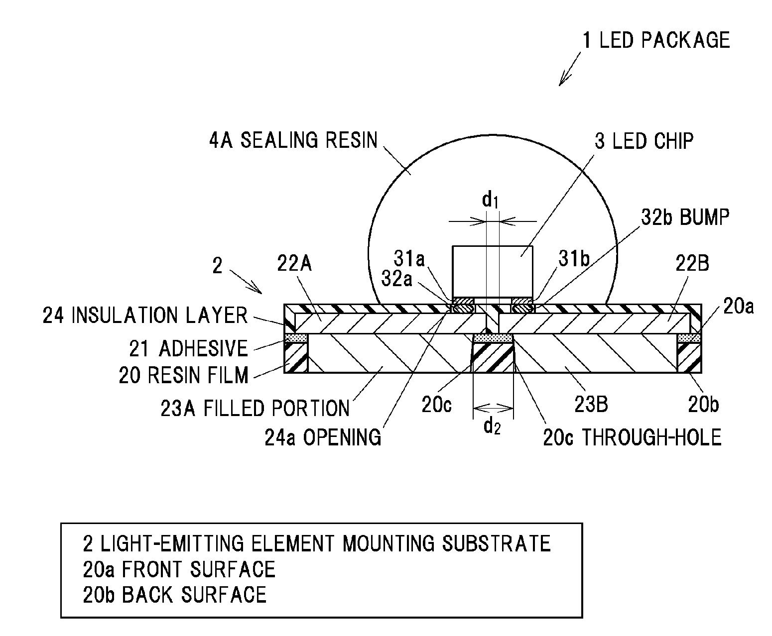
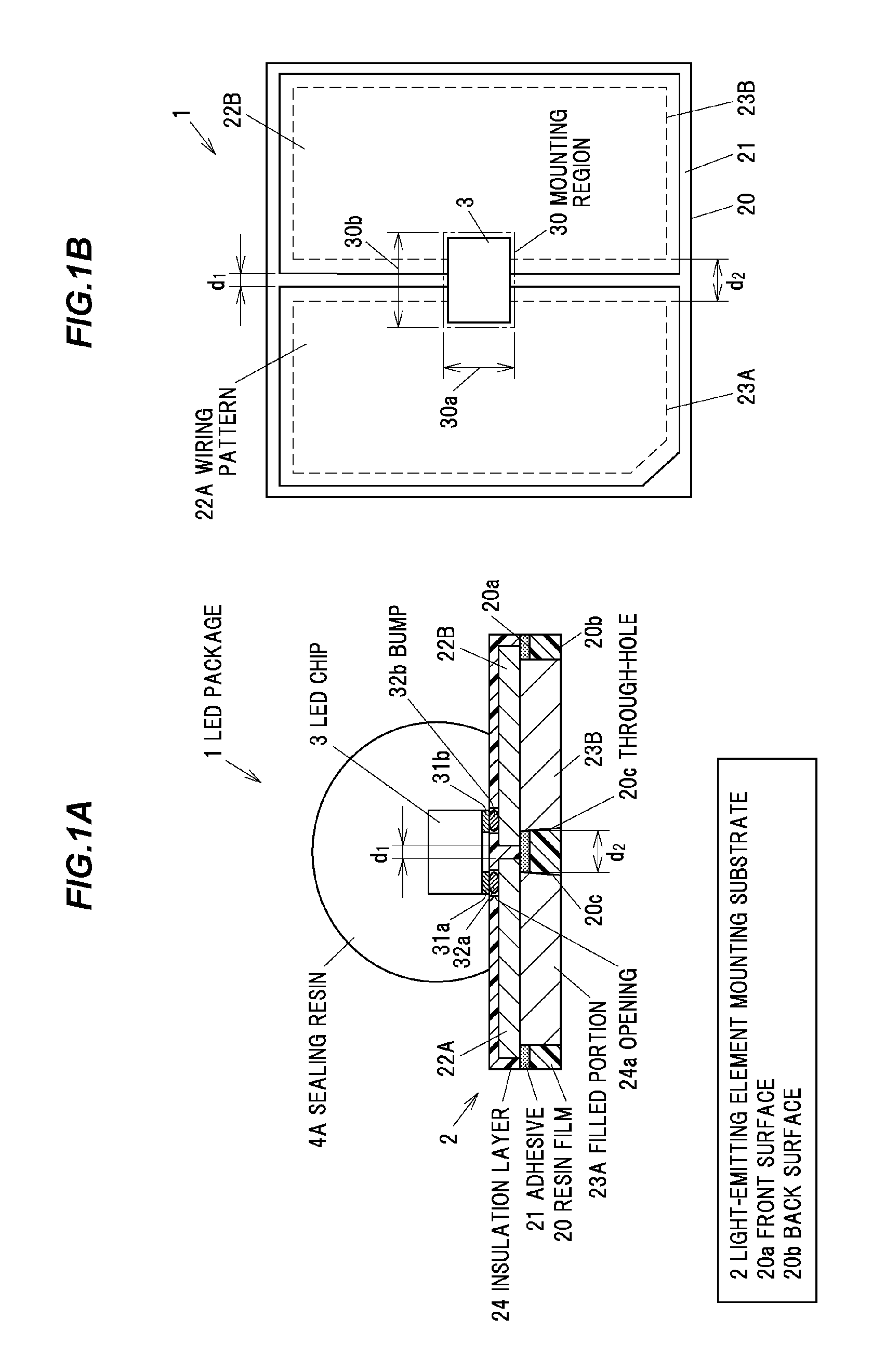
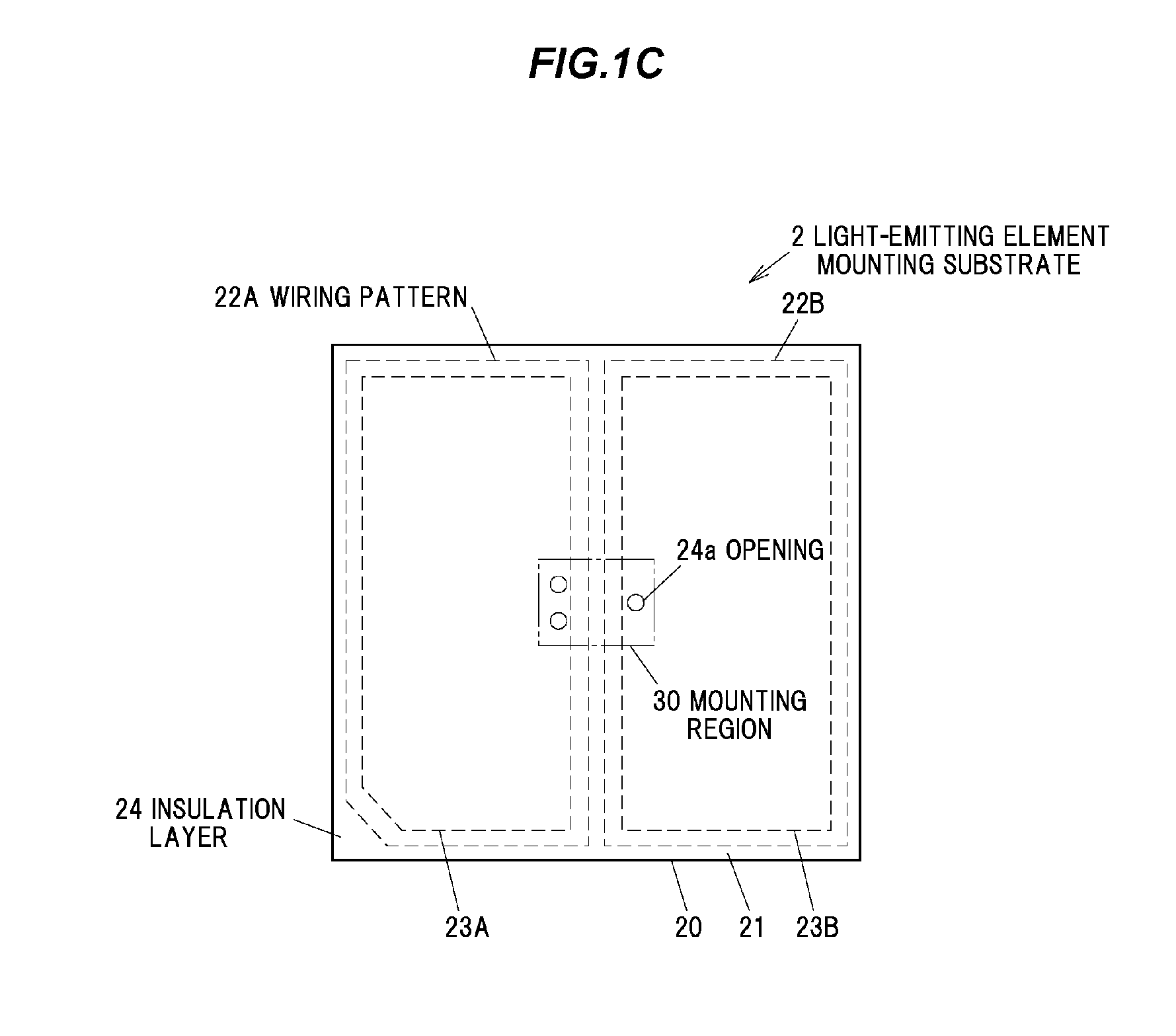
[0045]FIG. 1A is a cross sectional view showing an LED package in a first embodiment of the invention and FIG. 1B is a plan view showing the LED package of FIG. 1A without sealing resin and insulation layer. FIG. 1C is a plan view showing a light-emitting element mounting substrate.

[0046]As shown in FIGS. 1A and 1B, an LED package 1 as an example of a light-emitting device is configured such that a flip-chip type LED chip 3 having electrodes 31a and 31b on a bottom surface thereof is flip-chip mounted as a light-emitting element in a mounting region 30 of a pair of wiring patterns 22A and 22B on a light-emitting element mounting substrate 2 using bumps 32a and 32b for connection, and the LED chip 3 is then sealed with a sealing resin 4A.

[0047]The light-emitting element mounting substrate 2 is a so-called single-sided printed circuit board having a wiring on one surface of a substrate, and is provided with a resin film 20 as a substrate having insulating properties, a pair of wiring ...

second embodiment

[0117]FIG. 4A is plan view showing an LED package in a second embodiment of the invention without sealing resin and insulation layer and FIG4B is plan view showing a light-emitting element mounting substrate.

[0118]While one LED chip 3 is mounted on the light-emitting element mounting substrate 2 in the first embodiment, plural (e.g., three) LED chips 3 are mounted in the LED package 1 as shown in FIG. 4A in the second embodiment.

[0119]The mounting region 30 in the second embodiment is a region which includes three LED chips 3. The pair of wiring patterns 22A and 22B have the first distance d1 (e.g., 0.04 mm) not more than a length of the side 30b of the mounting region 30 in the range of not less than a length (e.g., 1.5 mm) of the side 30a of the mounting region 30.

[0120]The pair of filled portions 23A and 23B have the second distance d2 not more than a length (e.g., 0.3 mm) of the side 30b of the mounting region 30 in the range of not less than a length (e.g., 1.5 mm) of the side ...

third embodiment

[0122]FIG. 5A is plan view showing an LED package in a third embodiment of the invention without sealing resin and insulation layer and FIG. 5B is plan view showing a light-emitting element mounting substrate.

[0123]While only the flip-chip type LED chip(s) 3 is / are mounted in one mounting region 30 in the first and second embodiments, the LED chip(s) 3 as well as another electronic component are mounted in plural mounting regions 30A and 30B in the third embodiment.

[0124]That is, in the LED package 1 of the third embodiment, the mounting region 30A is provided on the pair of wiring patterns 22A and 22B in a bridging manner and the mounting region 30B is provided only on the wiring pattern 22A, as shown in FIG. 5A. This LED package 1 is configured such that the same flip-chip type LED chip 3 as the first and second embodiments is mounted on the mounting region 30A, a wire-bonding type LED chip 5A is mounted in the other mounting region 30B and a Zener diode 7 as an electrostatic brea...


PUM


Abstract

A light-emitting element mounting substrate includes an insulative substrate including a single-sided printed circuit board, a pair of wiring patterns formed on one surface of the substrate, the wiring patterns being separated with a first distance, a pair of filled portions including a metal filled in a pair of through-holes to contact the pair of wiring patterns and to be exposed on a surface of the substrate opposite to the one surface, the pair of through-holes being formed to penetrate through the substrate in a thickness direction and to be separated with a second distance, and an insulation layer having a light reflectivity formed on the one surface of the substrate. The pair of filled portions each have a horizontal projected area of not less than 50% of each area the pair of wiring patterns, and the insulation layer includes an opening to expose the pair of wiring patterns.

Description

[0001]The present application is based on Japanese patent application Nos. 2011-144546 and 2012-064702 filed on Jun. 29, 2011 and Mar. 22, 2012, respectively, the entire contents of which are incorporated herein by reference.BACKGROUND OF THE INVENTION[0002]1. Field of the Invention[0003]The invention relates to a light-emitting element mounting substrate and an LED package using the light-emitting element mounting substrate.[0004]2. Related Art[0005]In recent years, display devices and illuminating devices using an LED (Light Emitting Diode) chip as a light-emitting element have attracted attention from the viewpoint of energy saving, which enhances competition of developing LED chips and products or technologies related thereto at a global level. As a symbolic example, even a rate per unit luminosity (yen / 1 m) is well known as an index. Considering this unit, reduction of the rate per unit or an increase in luminous flux per unit is required in order to be competitive.[0006]In suc...

Claims


Application Information

Patent Timeline
Patent Type & Authority Applications(United States)
IPC IPC(8): H01L33/62
CPCH01L25/0753H01L25/167H01L33/48H01L33/60H01L33/62H01L2224/48091H01L2224/48137H01L2224/45144H01L2224/48227H01L2924/00014H01L2924/00
Inventor IMAI, NOBORUISAKA, FUMIYANEMOTO, MASANORITANOI, MINORUTAKAHASHI, TAKESHI
Owner SHINDO DENSHI KOGYO KK
Why Eureka
Try Eureka