
Canary based SRAM adaptive voltage scaling (AVS) architecture and canary cells for the same

a technology of adaptive voltage scaling and canary cells, applied in the field of memory banks, can solve the problems of power consumption of the soc, limited vdd scaling during dynamic operation of the memory, and limited power supply reduction

Active Publication Date: 2013-01-03
STMICROELECTRONICS INT NV
View PDF3 Cites 21 Cited by
  • Summary
  • Abstract
  • Description
  • Claims
  • Application Information

AI Technical Summary

Benefits of technology

The patent describes a memory bank with additional cells that can determine the operating voltage of the bank. These additional cells have a lower operating margin than the memory cells, which means they are less tolerant to device mismatches. The additional cells can also be selectively applied masks to adjust their operating parameters. The method for setting the operating voltage involves adjusting the supply voltage and checking the operation's success. The patent also describes a system that can detect failures in the memory and adjust the operating voltage accordingly. The technical effects of this patent are improved reliability and efficiency of the memory bank.

Problems solved by technology

Power consumption of the memory in both static and dynamic operation may, therefore, dominate the power consumed by the SoC.
However, due to the necessity to perform read and write operations, Vdd scaling during dynamic operation of the memory may be limited by the requirements for performing these operations without error.
Vdd scaling during standby or static operation may not be limited by the same constraints as the dynamic operation of the SRAM; however, the power supply reduction may still be limited by a minimum data retention voltage of a SRAM cell.
Designing for these Vdd scaling constraints for a SRAM may be difficult, because the Vdd scaling limits as found on a typical computer-aided design may be pessimistic as compared to the actual conditions of a silicon-implemented SoC.
This is because the computer aided design takes into account all of the process, temperature and supply variations, as well as the potential device mismatch.
However, although such adaptive voltage scaling techniques exist for standard cell logic, there is limited implementation for an embedded SRAM.
Consequently, it does not take into account the constraints imposed by the dynamic read and write operation of a SRAM.
The tunable replica bits may be limited in their application.

Method used


Image

  • Canary based SRAM adaptive voltage scaling (AVS) architecture and canary cells for the same
  • Canary based SRAM adaptive voltage scaling (AVS) architecture and canary cells for the same
  • Canary based SRAM adaptive voltage scaling (AVS) architecture and canary cells for the same

Examples


Embodiment Construction

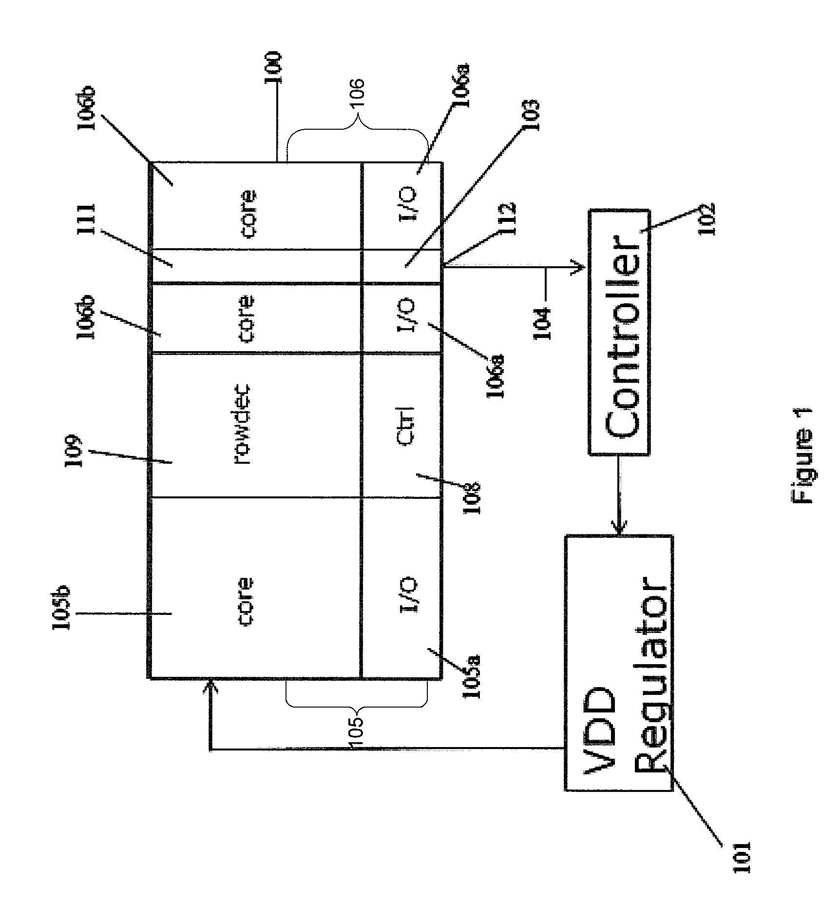
[0032]Some embodiments may relate, but not exclusively to, adaptive voltage scaling techniques implemented on on-chip memory. By way of example only some embodiments may relate to static random access memory SRAM in a system on a chip SoC and canary adaptive voltage scaling applied thereto.

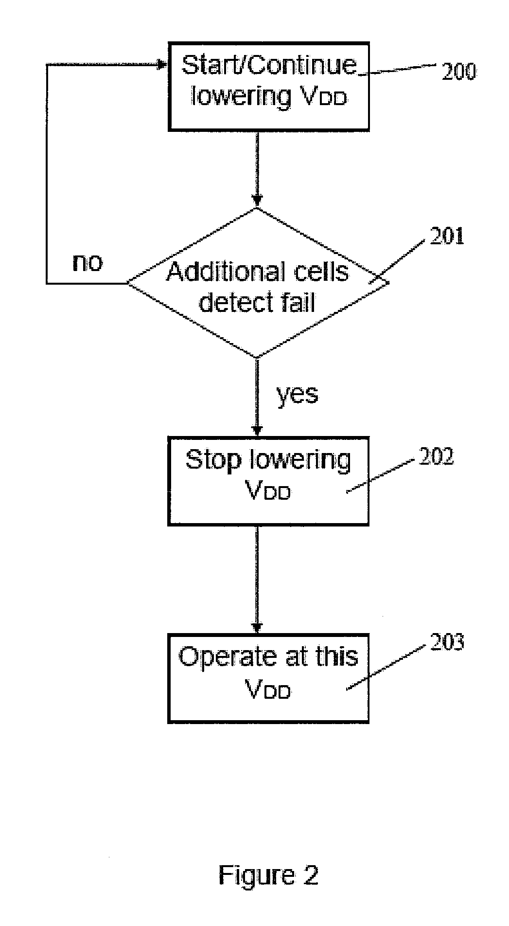
[0033]Embodiments may provide adaptive voltage scaling for memory. The memory may be, for example, SRAM or cache memory. The memory may form, for example, part of an embedded system or SoC. In embodiments, adaptive voltage scaling may be applied in a dynamic operation of memory cells. Some embodiments may provide adaptive voltage scaling for dynamic operation of memory cells, static operation of memory cells or dynamic and static operation of memory cells.

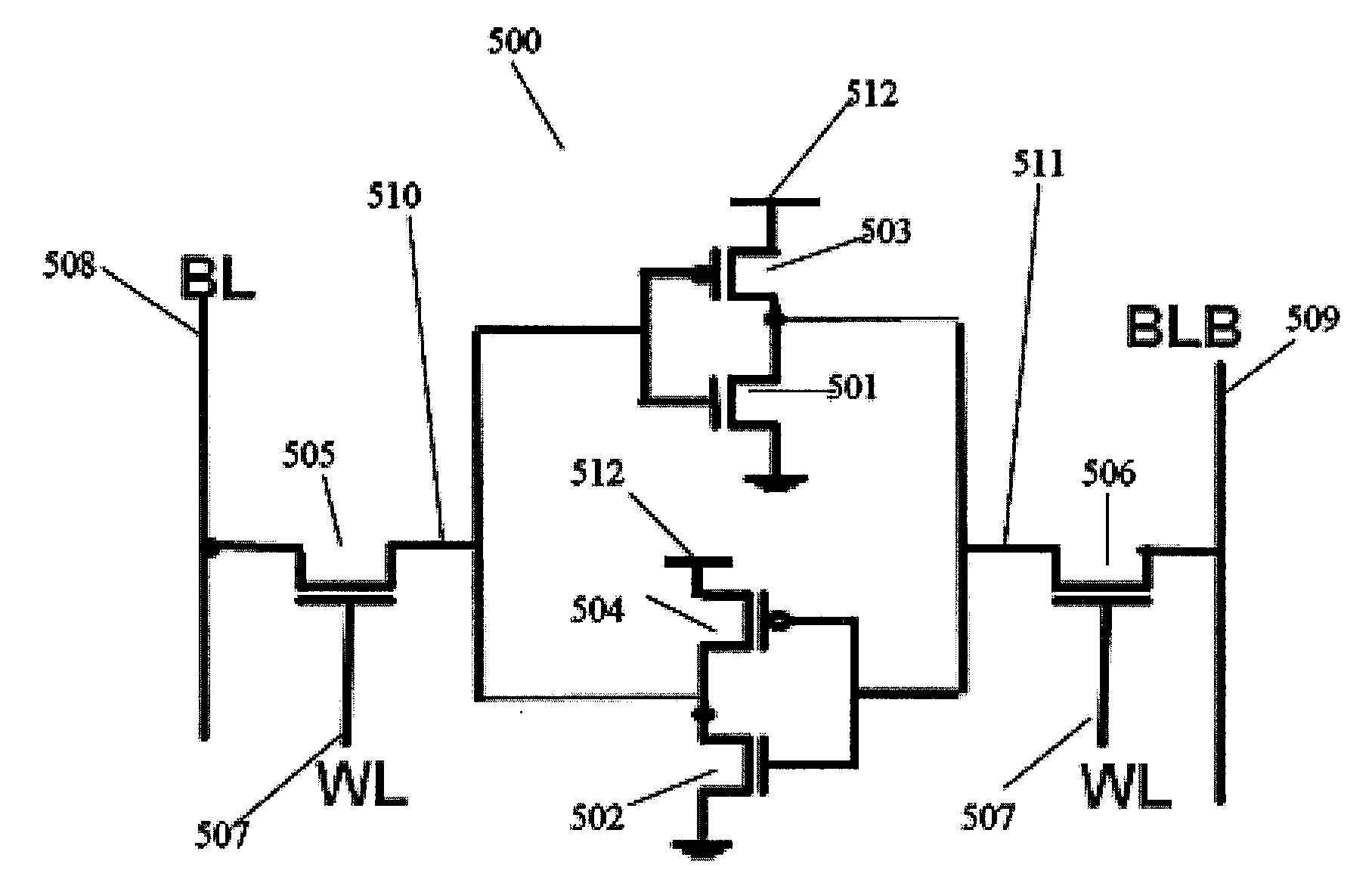
[0034]Embodiments may provide adaptive voltage scaling through use of additional cells. In some embodiments, the additional cells may be sensor cells for sensing; for example, a feedback to an adaptive voltage controller. In some embodiments, the...


PUM


Abstract

A memory bank includes memory cells and an additional cell to determine an operating voltage of the memory bank. The additional cell has an operating margin that is less than a corresponding operating margin of the other memory cells in the memory bank.

Description

FIELD OF THE INVENTION[0001]The present invention relates to a memory bank. Particularly, but not exclusively, some embodiments of the present invention relate to setting an operational voltage for a memory bank.BACKGROUND OF THE INVENTION[0002]SRAM or cache memory on a system-on-chip SoC may occupy a large portion of the SoC. Typically, this might be between 50 and 60%. Power consumption of the memory in both static and dynamic operation may, therefore, dominate the power consumed by the SoC.[0003]In order to increase power efficiency of the SoC, attempts have been made to reduce SRAM leakage components and dynamic power by power supply Vdd scaling. Dynamic voltage and frequency scaling (DVFS) may also be applied where the system frequency is lowered in the lower voltage operation mode.[0004]However, due to the necessity to perform read and write operations, Vdd scaling during dynamic operation of the memory may be limited by the requirements for performing these operations without...

Claims


Application Information

Patent Timeline
Patent Type & Authority Applications(United States)
IPC IPC(8): G11C11/00G11C8/00
CPCG11C5/147G11C11/417
Inventor ASTHANA, VIVEK
Owner STMICROELECTRONICS INT NV
Learn More