Apparatus and method for treating substrate

Active Publication Date: 2013-01-31
SEMES CO LTD
View PDF6 Cites 2 Cited by
  • Summary
  • Abstract
  • Description
  • Claims
  • Application Information

AI Technical Summary

Benefits of technology

[0007]The present invention provides an apparatus and method for treating a substrate

Problems solved by technology

During such processes, contaminants such as particles, organic contaminants, and metallic impurities are generated, which cause defects on a substrate and affect the yield of semiconductor device manufacturing processes.
However, semiconductor devices having fine circuit patterns are not satisfactorily dried,

Method used


Image

  • Apparatus and method for treating substrate
  • Apparatus and method for treating substrate
  • Apparatus and method for treating substrate

Examples


Example

[0046]In the following description, terms and drawings are used for explaining embodiments of the present invention while not limiting the present invention.

[0047]Known techniques used in the present invention but not related to the concept of the present invention will not be explained in detail.

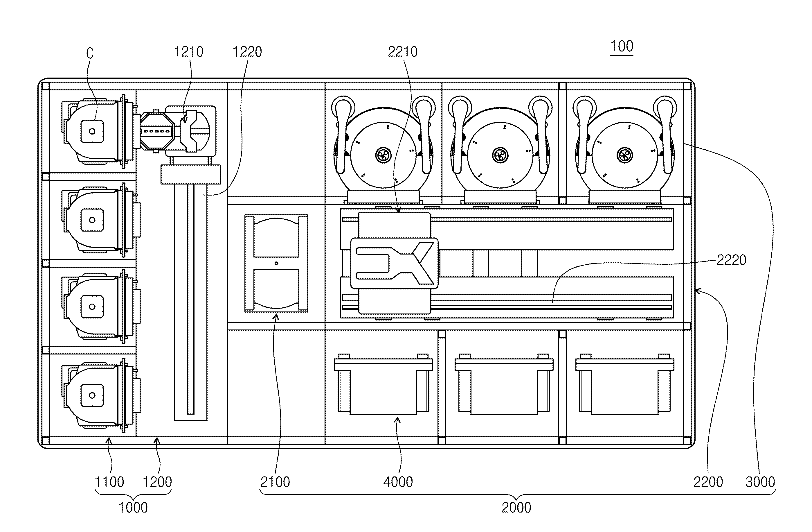
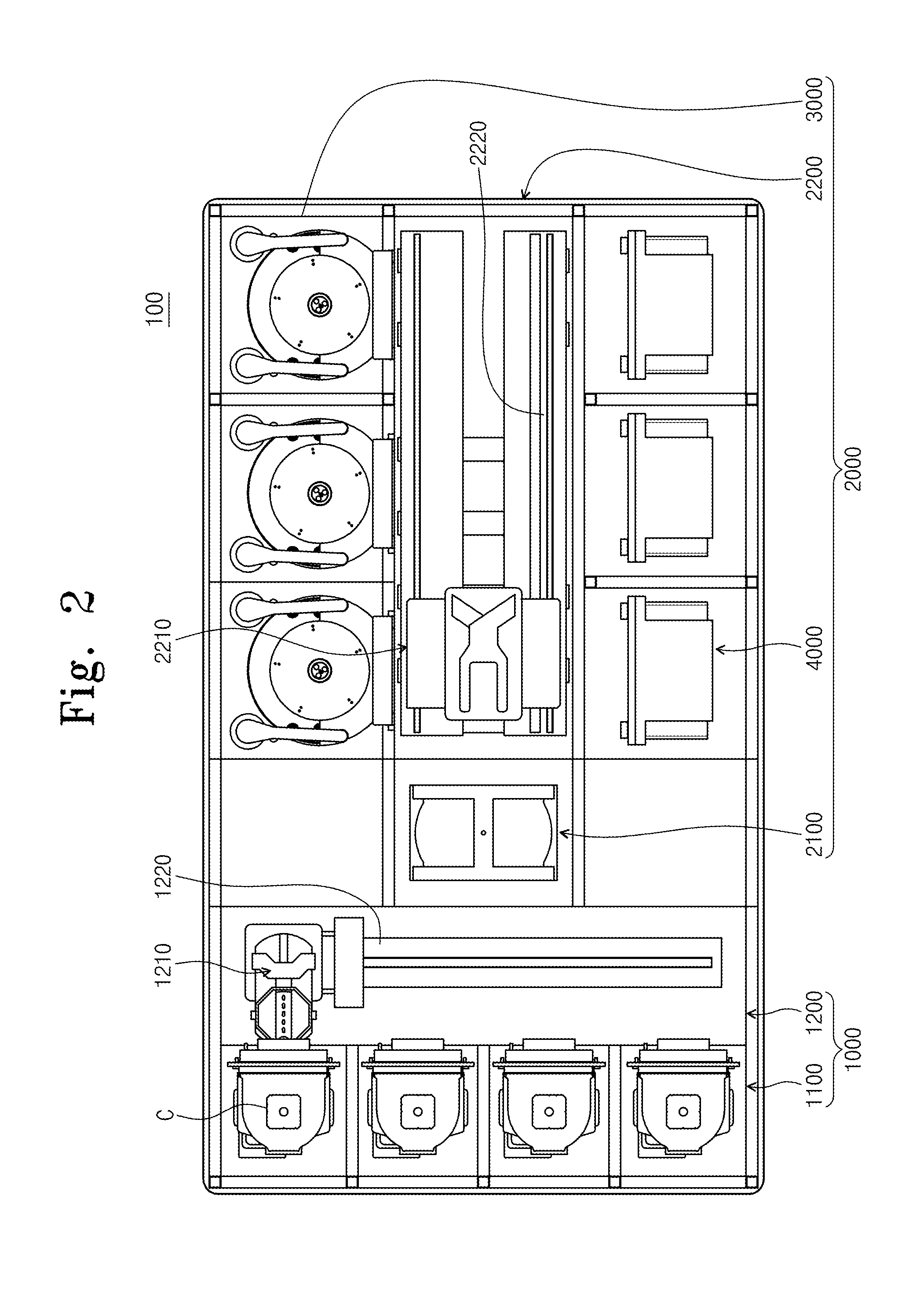
[0048]Hereinafter, a substrate treating apparatus 100 will be described according to exemplary embodiments of the present invention.

[0049]The substrate treating apparatus 100 may be used to perform a supercritical process for treating a substrate (S) using a supercritical fluid as a process fluid.

[0050]The term “substrate (S)” is used herein to denote any substrate used to manufacture a product such as a semiconductor device and a flat panel display (FPD) in which circuit patterns are formed on a thin film. Examples of substrates (S) include wafers such as silicon wafers, glass substrates, and organic substrates.

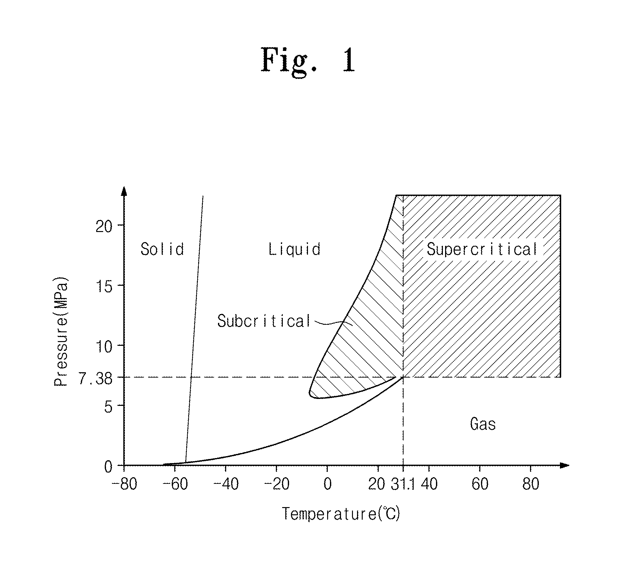
[0051]The term “supercritical fluid” means any substance having both the gas an...


PUM


Abstract

Provided are an apparatus and method for treating a substrate. More particularly, an apparatus and method for treating a substrate through a supercritical process are provided. The apparatus includes: a housing having an entrance in a predetermined surface thereof and providing a space for performing a high pressure process; a support member disposed in the housing to support a substrate; a door for opening and closing the entrance; and a pressing member configured to apply a force to the door so as to close the housing during the high pressure process.

Description

CROSS-REFERENCE TO RELATED APPLICATIONS[0001]This U.S. non-provisional patent application claims priority under 35 U.S.C. §119 of Korean Patent Application Nos. 10-2011-0076240, filed on Jul. 29, 2011, and 10-2011-0140008, filed on Dec. 22, 2011, the entire contents of which are hereby incorporated by reference.BACKGROUND OF THE INVENTION[0002]The present invention disclosed herein relates to an apparatus and method for treating a substrate, and more particularly, to an apparatus and method for treating a substrate through a supercritical process.[0003]Semiconductor devices are manufactured by forming circuit patterns on a substrate through various processes such as a photolithography process. During such processes, contaminants such as particles, organic contaminants, and metallic impurities are generated, which cause defects on a substrate and affect the yield of semiconductor device manufacturing processes. Therefore, cleaning processes are included in semiconductor device manufa...

Claims


Application Information

Patent Timeline
IPC IPC(8): F27D7/02H01L21/677A47B87/02A47B96/00A47B87/00
CPCH01L21/67126F27B17/0025H01L21/6719H01L21/67178
Inventor PARK, JOO JIBKWON, OH JINJANG, SUNGHOKIM, BOONG
Owner SEMES CO LTD
Why Eureka
Try Eureka