

Chip-component structure
a chip and component technology, applied in the direction of fixed capacitor details, electrical apparatus construction details, stacked capacitors, etc., can solve the problem of difficult cleaning off, and achieve the effect of reducing the amount of joining materials and reducing audible noise in the circuit board
- Summary
- Abstract
- Description
- Claims
- Application Information
AI Technical Summary
Benefits of technology
Problems solved by technology
Method used
Image

Examples
first preferred embodiment
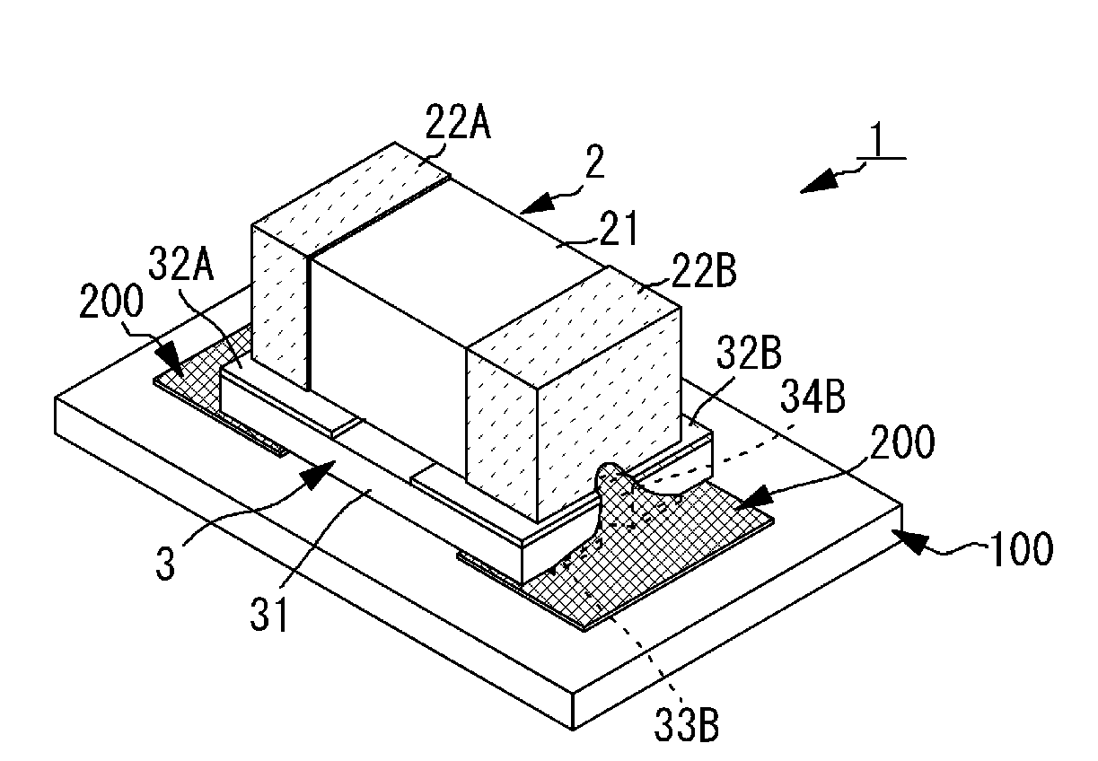
[0027]A chip-component structure 1 according to a first preferred embodiment of the present invention will be described below.
[0028]The chip-component structure 1 includes a multilayer capacitor 2 and an interposer 3. Details of the structures of the multilayer capacitor 2 and the interposer 3 will be described in detail below.
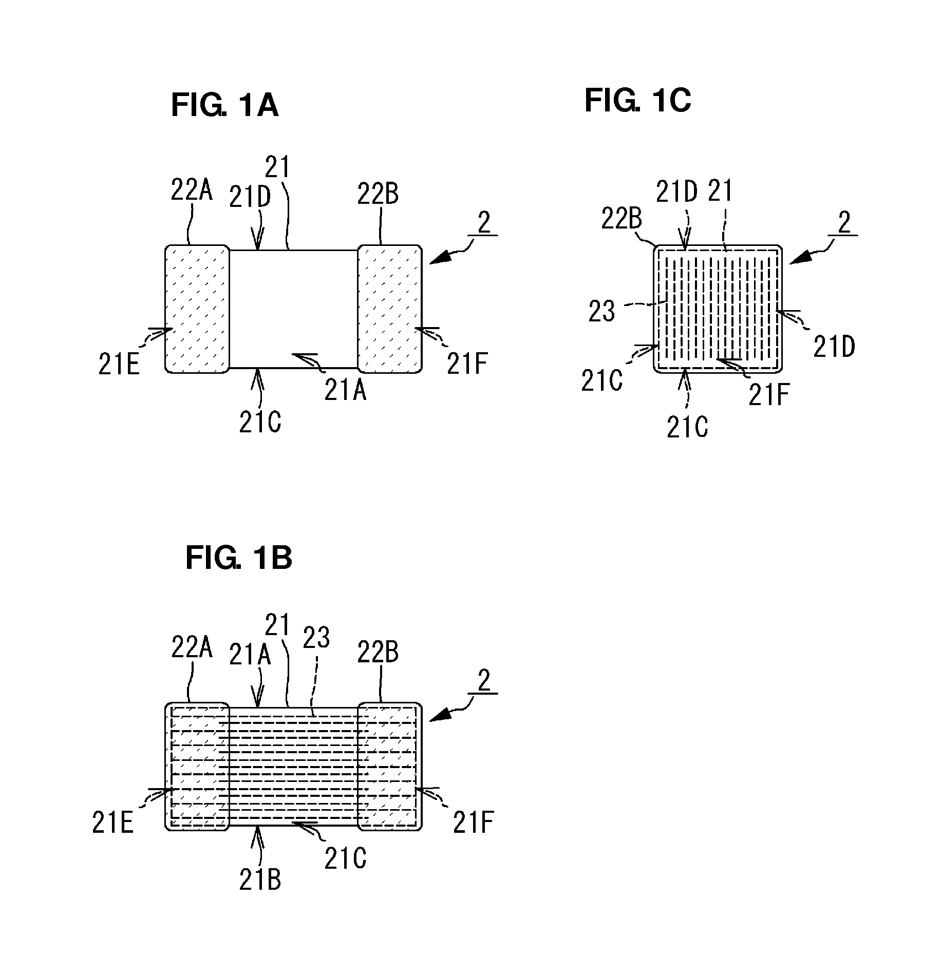
[0029]FIGS. 1A, 1B, and 1C are a plan view, a front view, and a right side view, respectively, of the multilayer capacitor 2.
[0030]The multilayer capacitor 2 includes a laminated body 21, external electrodes 22A and 22B, and internal electrodes 23.
[0031]The laminated body 21 preferably has a substantially rectangular parallelepiped outer shape including a top surface 21A, a bottom surface 21B, a front surface 21C, a back surface 21D, a left side surface 21E, and a right side surface 21F. The top surface 21A, the bottom surface 21B, the front surface 21C, and the back surface 21D are substantially rectangular, and are adjacent to one another at long sides. The ...
second preferred embodiment
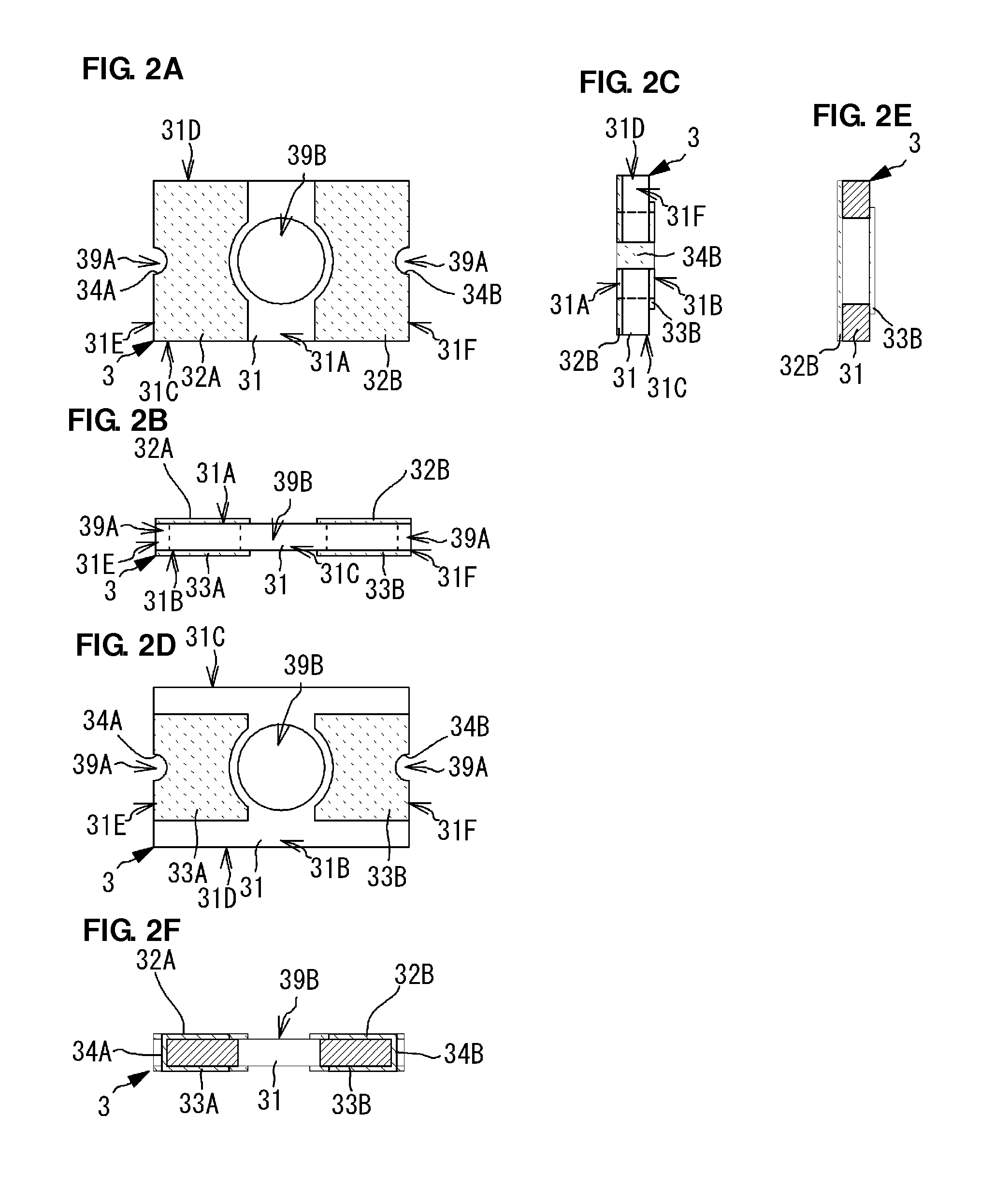
[0055]FIGS. 5A, 5B, and 5C are a plan view, a sectional front view, and a bottom view, respectively, of a chip-component structure 1A according to a second preferred embodiment.
[0056]The chip-component structure 1A of the second preferred embodiment is preferably the same in the structure of a multilayer capacitor 2 as the chip-component structure 1 of the first preferred embodiment, but is different in that an interposer 3A having a different size is included. For this reason, in the following description, structures corresponding to the structures adopted in the first preferred embodiment are denoted by the same reference numerals.
[0057]The outer shape of the interposer 3A in plan view is substantially identical to that of the multilayer capacitor 2. For this reason, arcs of grooves 39A provided in both longitudinal end surfaces of a substrate 31 are entirely located under bottom surfaces of external electrodes 22A and 22B of the multilayer capacitor 2.
[0058]In this structure, a c...
third preferred embodiment
[0061]FIGS. 6A, 6B, and 6C are a plan view, a sectional front view, and a bottom view, respectively, of a chip-component structure 1B according to a third preferred embodiment.
[0062]The chip-component structure 1B of the third preferred embodiment is the same in the structure of a multilayer capacitor 2 as the chip-component structure 1 of the first preferred embodiment, but is different in that an interposer 3B having a different size is included. For this reason, in the following description, structures corresponding to the structures adopted in the first preferred embodiment are denoted by the same reference numerals.
[0063]The interposer 3B has an area wider than that of the interposer 3 of the first preferred embodiment. Grooves 39A provided in both longitudinal end surfaces of a substrate 31 do not overlap with external electrodes 22A and 22B of the multilayer capacitor 2, as viewed in a principal-surface normal direction, and arcs thereof are exposed entirely.
[0064]In this str...
PUM
| Property | Measurement | Unit |
|---|---|---|
| Area | aaaaa | aaaaa |
| Depth | aaaaa | aaaaa |
Abstract
Description
Claims
Application Information