Output driving circuit and transistor output circuit

a driving circuit and output circuit technology, applied in the direction of oscillator generators, pulse techniques, instruments, etc., can solve problems such as the breakdown of the transistor device, and achieve the effect of stable operation and low current consumption

Inactive Publication Date: 2013-02-14
SAMSUNG ELECTRO MECHANICS CO LTD
View PDF2 Cites 4 Cited by
  • Summary
  • Abstract
  • Description
  • Claims
  • Application Information

AI Technical Summary

Benefits of technology

[0011]To overcome this problem, an object of the present invention is to provide an output driving circuit and a transistor output circuit, which may include a level shift unit and may stably operate when a high voltage that is smaller than a source-drain breakdown voltage and is greater than a gate-source breakdown voltage is applied to a gate of the output transistor.
[0012]Another object of the present invention is to provide an output driving circuit and a transistor output circuit, which may include a level shift unit for stably operating an output transistor at a high frequency and for stably operating an output transistor at a low amount of current consumed.

Problems solved by technology

In this case, since the power voltage is greater than the source-gate breakdown voltage BVsg, the transistor device may breakdown.

Method used


Image

  • Output driving circuit and transistor output circuit
  • Output driving circuit and transistor output circuit
  • Output driving circuit and transistor output circuit

Examples


Embodiment Construction

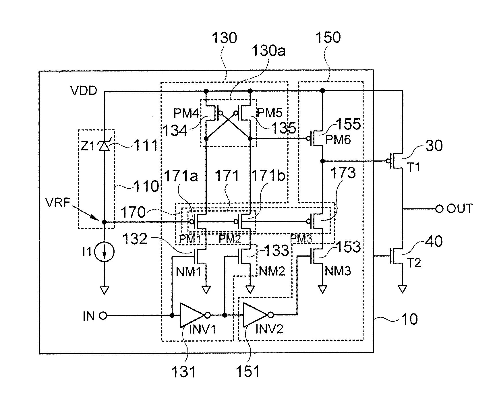
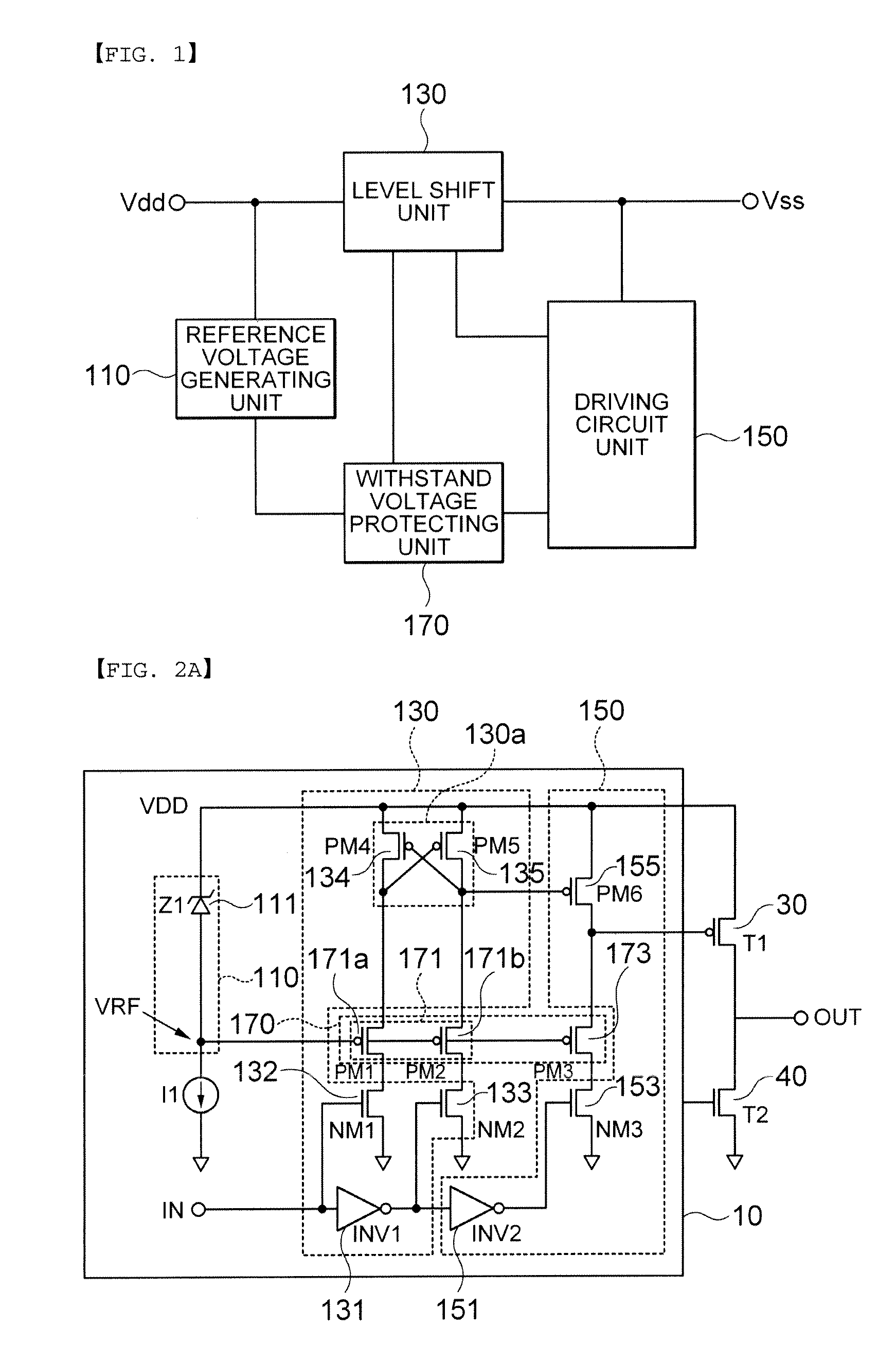
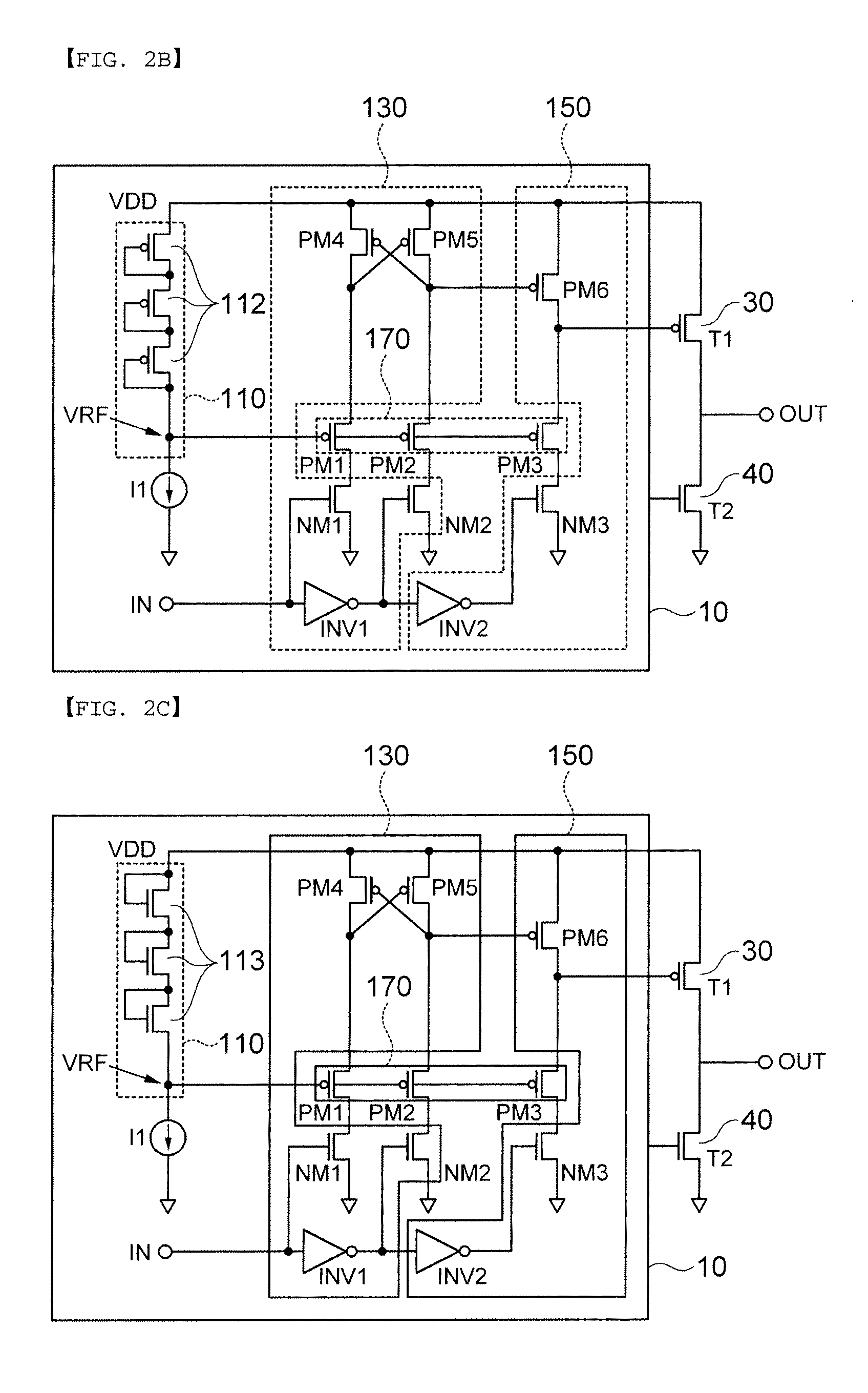
[0028]Exemplary embodiments of the present invention for accomplishing the above-mentioned objects will be described with reference to the accompanying drawings. In describing exemplary embodiments of the present invention, the same reference numerals will be used to describe the same components and an additional description that is overlapped or allow the meaning of the present invention to be restrictively interpreted will be omitted.

[0029]It will be understood that when an element is simply referred to as being ‘connected to’ or ‘coupled to’ another element without being ‘directly connected to’ or ‘directly coupled to’ another element in the present description, it may be ‘directly connected to’ or ‘directly coupled to’ another element or be connected to or coupled to another element, having the other element intervening therebetween.

[0030]Although a singular form is used in the present description, it may include a plural form as long as it is opposite to the concept of the pres...


PUM


Abstract

Disclosed herein are an output driving circuit and a transistor output circuit. The output driving circuit includes: a reference voltage generating unit generating a reference voltage; a level shift unit including a transistor latch and turning off a first transistor of a driving circuit or driving the first transistor; a driving circuit unit including the first transistor that is driven to apply power to a gate of an output transistor and a second transistor that is driven complementarily to the first transistor to lower a gate voltage of the output transistor and drive the output transistor; and an withstand voltage protecting unit that is driven by receiving a reference voltage and includes a first withstand voltage protecting unit for protecting transistors of the transistor latch and the first transistor for stable operations thereof and a second withstand voltage protecting unit for protecting the output transistor for a stable operation thereof.

Description

CROSS REFERENCE(S) TO RELATED APPLICATIONS[0001]This application claims the benefit under 35 U.S.C. Section 119 of Korean Patent Application Serial No. 10-2011-0079171, entitled “Output Driving Circuit and Transistor Output Circuit” filed on Aug. 9, 2011, which is hereby incorporated by reference in its entirety into this application.BACKGROUND OF THE INVENTION[0002]1. Technical Field[0003]The present invention relates to an output driving circuit and a transistor output circuit, and more particularly, to an output driving circuit and a transistor output circuit that stably operate when a high voltage that is smaller than a source-drain breakdown voltage and is greater than a gate-source breakdown voltage is applied to a gate of an output transistor.[0004]2. Description of the Related Art[0005]An operating voltage of a P-channel transistor, for example a P-channel LDMOS is determined according to a source-drain breakdown voltage BVsd, a source-gate breakdown voltage BVsg, and a gate...

Claims


Application Information

Patent Timeline
Patent Type & Authority Applications(United States)
IPC IPC(8): H03K3/00
CPCH03K17/08122H03K3/356104G05F3/02G05F3/24
Inventor HEO, CHANG JAE
Owner SAMSUNG ELECTRO MECHANICS CO LTD
Why Eureka
Try Eureka