Semiconductor device packaging having pre-encapsulation through via formation

a technology of semiconductor devices and vias, which is applied in the direction of solid-state devices, printed circuit manufacture, basic electric elements, etc., can solve the problems of high cost of materials, process and additional tooling to generate through vias

Inactive Publication Date: 2013-02-28
FREESCALE SEMICON INC
View PDF5 Cites 96 Cited by
  • Summary
  • Abstract
  • Description
  • Claims
  • Application Information

AI Technical Summary

Problems solved by technology

This process of post-encapsulation via formation introduces complexities to the manufacturing process that have a variety of manufacturing and reliability challenges (e.g., consisten...

Method used


Image

  • Semiconductor device packaging having pre-encapsulation through via formation
  • Semiconductor device packaging having pre-encapsulation through via formation
  • Semiconductor device packaging having pre-encapsulation through via formation

Examples


Embodiment Construction

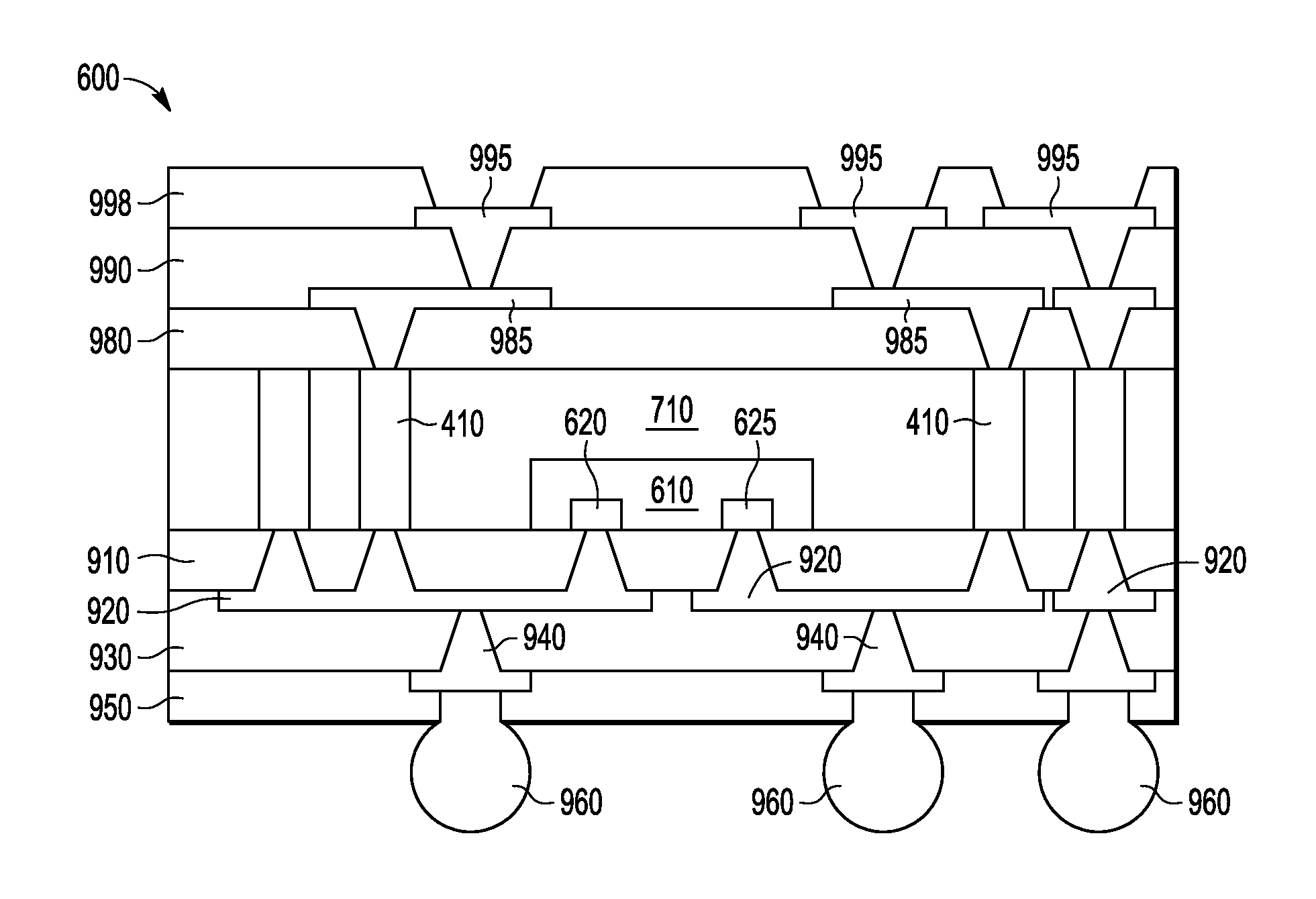
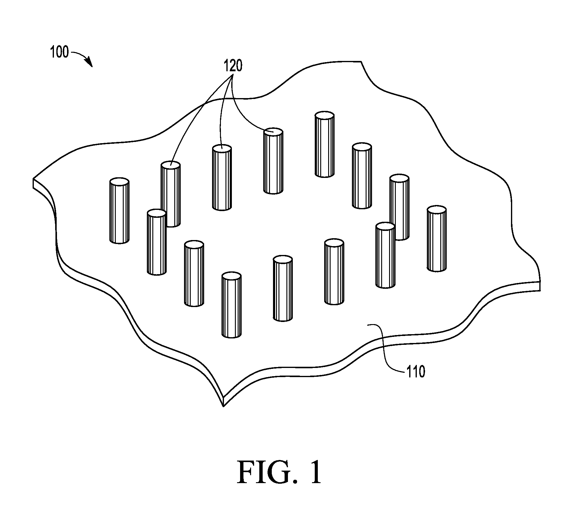
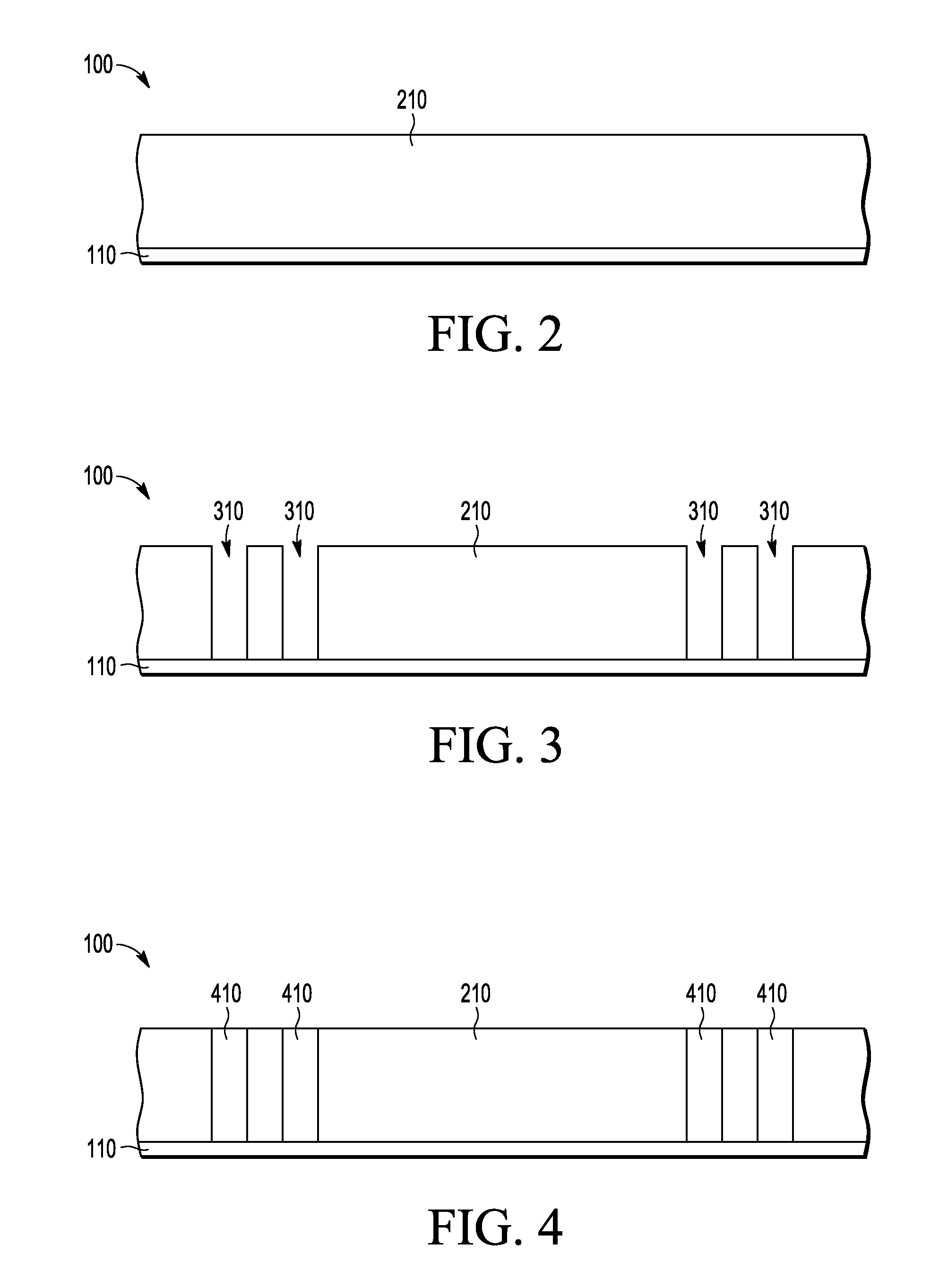
[0019]A method for forming signal conduits before encapsulation for incorporation as through vias in a semiconductor device package is provided. One or more signal conduits are formed through photolithography and metal deposition on a metal film or substrate. After removing photoresistive material, the semiconductor device package is built by encapsulating the signal conduits along with any semiconductor die and other parts of the package. The ends of the signal conduits are exposed and the signal conduits can then be used as through vias, providing signal-bearing pathways between interconnects or contacts on the bottom and top of the package, and electrical contacts of the semiconductor die. Using this method, signal conduits can be provided in a variety of geometric placings in the semiconductor device package.

[0020]For convenience of explanation, and not intended to be limiting, the present invention is described for semiconductor devices, but persons of skill in the art will und...


PUM


Abstract

A method for forming signal conduits before encapsulation for incorporation as through vias in a semiconductor device package is provided. One or more signal conduits are formed through photolithography and metal deposition on a metal film or substrate. After removing photoresistive material, the semiconductor device package is built by encapsulating the signal conduits along with any semiconductor die and other parts of the package. The ends of the signal conduits are exposed and the signal conduits can then be used as through vias, providing signal-bearing pathways between interconnects or contacts on the bottom and top of the package, and electrical contacts of the semiconductor die. Using this method, signal conduits can be provided in a variety of geometric placings in the semiconductor device package. A semiconductor device package including the signal conduits made from the above method is also provided.

Description

CROSS-REFERENCE TO RELATED APPLICATIONS[0001]This application is related to U.S. patent application Ser. No. ______ (Attorney Docket No. MT11599ZK), filed on even date, entitled “SEMICONDUCTOR DEVICE PACKAGING HAVING PRE-ENCAPSULATION THROUGH VIA FORMATION USING LEAD FRAMES WITH ATTACHED SIGNAL CONDUITS,” naming Zhiwei Gong, Navjot Chhabra, Glenn G. Daves, and Scott M. Hayes as inventors, and assigned to the current assignee hereof and U.S. patent application Ser. No. ______ (Attorney Docket No. MT1600ZK), filed on even date, entitled “SEMICONDUCTOR DEVICE PACKAGING HAVING PRE-ENCAPSULATION THROUGH VIA FORMATION USING DROP-IN SIGNAL CONDUITS,” naming Zhiwei Gong, Navjot Chhabra, Glenn G. Daves, and Scott M. Hayes, Douglas G. Mitchell, and Jason R. Wright as inventors, and assigned to the current assignee hereof.BACKGROUND[0002]1. Field[0003]This disclosure relates generally to semiconductor device packaging, and more specifically, to providing through-package vias in an encapsulated...

Claims


Application Information

Patent Timeline
IPC IPC(8): H01L21/77H01L21/56H01L23/48
CPCH01L24/19H01L2924/01012H01L2924/01029H01L23/3128H01L21/568H05K3/4602H05K2203/0733H01L24/96H01L2224/12105H05K1/185H01L2924/12042H01L2924/181H01L2924/00
Inventor GONG, ZHIWEICHHABRA, NAVJOTDAVES, GLENN G.HAYES, SCOTT M.
Owner FREESCALE SEMICON INC
Why Eureka
Try Eureka