Semiconductor package having plural semiconductor chips and method of forming the same

a technology of semiconductor chips and semiconductor chips, applied in the direction of semiconductor devices, semiconductor/solid-state device details, electrical apparatus, etc., can solve the problems of difficult to realize a thin package and operate at a high speed

Active Publication Date: 2013-02-28
SAMSUNG ELECTRONICS CO LTD
View PDF5 Cites 98 Cited by
  • Summary
  • Abstract
  • Description
  • Claims
  • Application Information

AI Technical Summary

Problems solved by technology

However, for at least some applications, conventional multi-chip packaging techniques...

Method used


Image

  • Semiconductor package having plural semiconductor chips and method of forming the same
  • Semiconductor package having plural semiconductor chips and method of forming the same
  • Semiconductor package having plural semiconductor chips and method of forming the same

Examples


Embodiment Construction

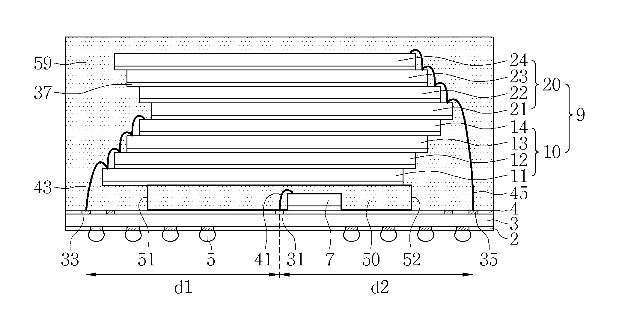
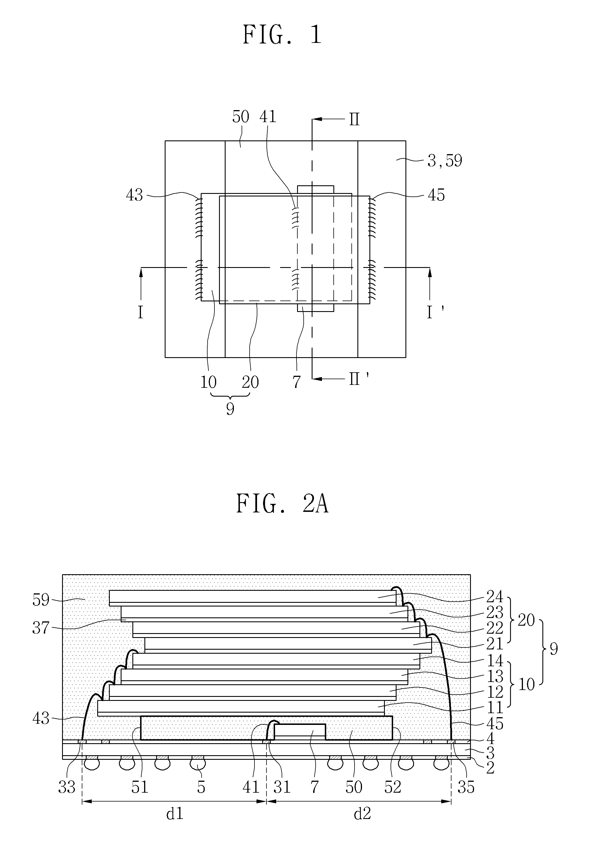
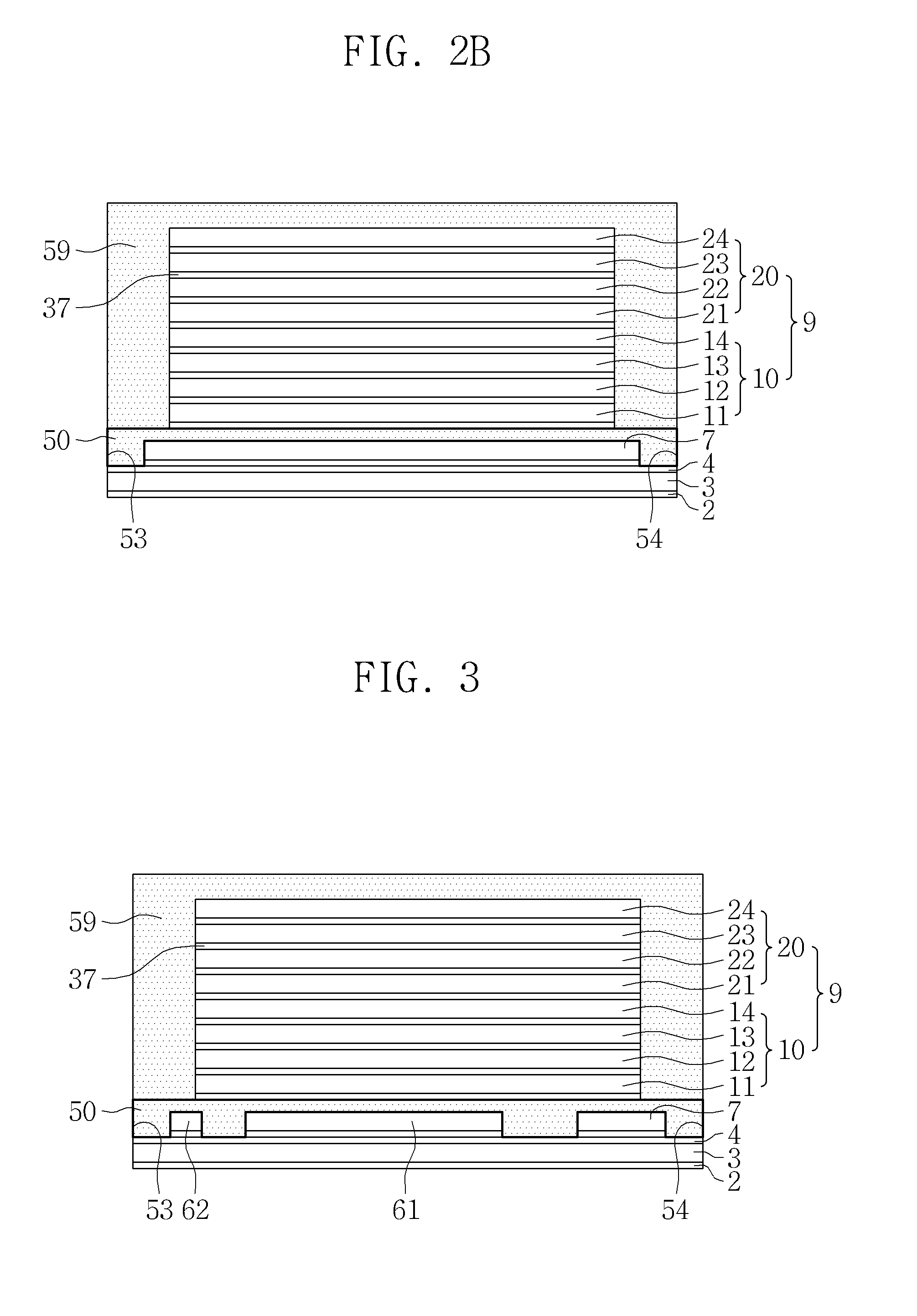
[0019]Various embodiments and examples of embodiments of the inventive concept will be described more fully hereinafter with reference to the accompanying drawings. In the drawings, the sizes and relative sizes and shapes of elements and layers shown in section may be exaggerated for clarity. In particular, the cross-sectional illustrations of the semiconductor devices and intermediate structures fabricated during the course of their manufacture are schematic. Also, like numerals are used to designate like elements throughout the drawings.

[0020]It will also be understood that when an element or layer in question is referred to as being “on” another element or layer, the element or layer in question can be directly on the other element or layer or an intervening element(s) or layer(s) may be present. Likewise, it will be understood that if an element or layer is referred to as being “connected” to another element or layer, the element or layer in question can be directly or indirectl...


PUM


Abstract

A semiconductor package includes a first semiconductor chip mounted to a substrate, a first encapsulant covering the first semiconductor chip and have first to fourth sidewall surfaces, and a chip stack mounted to the substrate and disposed on the first encapsulant. The chip stack includes a plurality of second semiconductor chips. A second encapsulant covers the chip stack. The second encapsulant may cover the first sidewall surface of the first encapsulant and expose the third sidewall surface of the first encapsulant.

Description

PRIORITY STATEMENT[0001]This application claims priority under 35 U.S.C. §119 to Korean Patent Application No. 10-2011-0088093 filed on Aug. 31, 2011, the disclosure of which is hereby incorporated by reference in its entirety.BACKGROUND[0002]1. Field[0003]The inventive concept relates to semiconductor packages having a plurality of semiconductor chips and to methods of manufacturing the same. More specifically, the inventive concept relates to a semiconductor package having stacked semiconductor chips and to a method of manufacturing the same.[0004]2. Description of Related Art[0005]Today's semiconductor packages must be small and yet provide a large capacity to store and / or process data in order to meet the current demand for light, thin, and compact mobile devices which are also multi-functional. A technique of stacking chips has been used to provide semiconductor packages that provide a large capacity to store and / or process data.[0006]A basic chip stacking technique includes st...

Claims


Application Information

Patent Timeline
IPC IPC(8): H01L23/28H01L23/48
CPCH01L23/3128H01L23/3135H01L21/561H01L2224/48145H01L24/97H01L2224/32145H01L2224/32225H01L2224/48227H01L2224/73265H01L2224/45124H01L2224/45144H01L2224/16145H01L2224/16225H01L2224/73204H01L2924/15311H01L2224/97H01L25/03H01L25/50H01L2225/0651H01L2225/06513H01L2225/06506H01L2225/06541H01L2225/06562H01L2924/00H01L2924/00012H01L24/73H01L2224/73253H01L2924/181H01L2924/19105H01L23/12H01L23/28
Inventor HAN, CHANG-HOONKIM, JIN-HOKIM, BO-SEONGOH, YUN-JIN
Owner SAMSUNG ELECTRONICS CO LTD
Why Eureka
Try Eureka