Semiconductor Device and Manufacturing Method Thereof

Active Publication Date: 2013-03-14
SEMICONDUCTOR MANUFACTURING INTERNATIONAL (BEIJING) CORP
View PDF3 Cites 7 Cited by
  • Summary
  • Abstract
  • Description
  • Claims
  • Application Information

AI Technical Summary

Benefits of technology

[0035]An advantage of the present invention is in that through depositing a stop layer on the bottom electrode, the chemical mechanical polishing process for planarizing the first insulating layer and removing the upper horizontal portion of the bottom electrode can be divided into two stages. The first stage terminates at the stop layer. Polishing time can be easily controlled even if the first insulating layer is relatively thick. It is only needed to remove the upper horizontal portion of the bottom electrode and the stop layer thereon in the second stage. The stop la

Problems solved by technology

As a result, it is difficult to accurately control the polishing time to stop polishing process imm

Method used


Image

  • Semiconductor Device and Manufacturing Method Thereof
  • Semiconductor Device and Manufacturing Method Thereof
  • Semiconductor Device and Manufacturing Method Thereof

Examples


Example

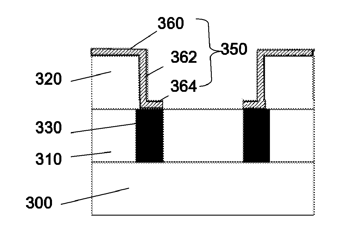
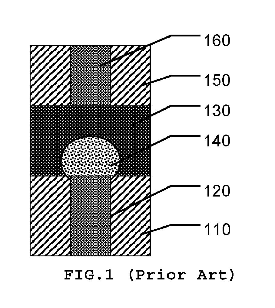
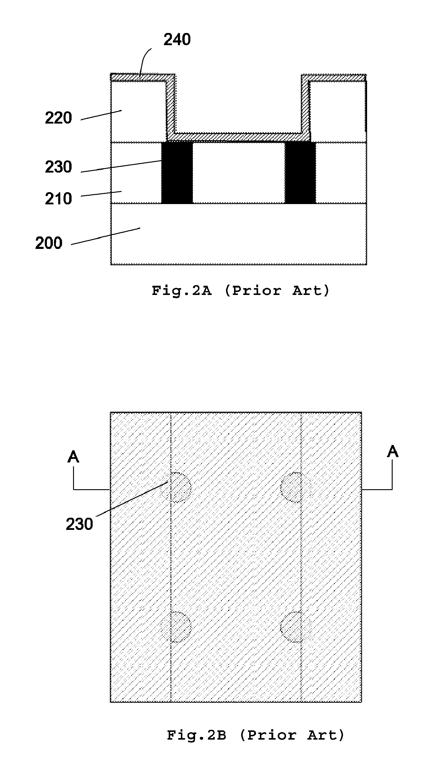
[0043]Various exemplary embodiments of the present invention will now be described in detail with reference to the drawings. It should be noted that the relative arrangement of the components and steps, the numerical expressions, and numerical values set forth in these embodiments do not limit the scope of the present invention unless it is specifically stated otherwise.

[0044]At the same time, it should be appreciated that for the convenience of description, the sizes of respective components in these figures may not be drawn based on actual scale.

[0045]The following description of at least one exemplary embodiment is merely illustrative in nature and is in no way intended to limit the invention, its application, or uses.

[0046]Techniques, methods and apparatus as known by one of ordinary skill in the relevant art may not be discussed in detail but are intended to be part of the specification where appropriate.

[0047]In all of the examples illustrated and discussed herein, any specifi...


PUM


Abstract

This invention discloses a semiconductor device and its manufacturing method. According to the method, a stop layer is deposited on a step-shaped bottom electrode, and then a first insulating layer is deposited through a high aspect ratio process. A first chemical mechanical polishing is performed until the stop layer. A second chemical mechanical polishing is then performed to remove the upper horizontal portion of the bottom electrode. Then, a phase-change material can be formed on the vertical portion of the bottom electrode to form a phase-change element. Through arranging a stop layer, the chemical mechanical polishing process is divided into two stages. Thus, during the second chemical mechanical polishing process preformed on the bottom electrode, polishing process can be precisely controlled to avoid the unnecessary loss of the bottom electrode.

Description

CROSS-REFERENCE TO RELATED APPLICATIONS[0001]This application claims priority to Chinese Patent Application No. 201110270585.5, filed on Sep. 14, 2011 and entitled “SEMICONDUCTOR DEVICE AND MANUFACTURING METHOD THEREOF”, which is incorporated herein by reference in its entirety.BACKGROUND OF THE INVENTION[0002]1. Field of the Invention[0003]The present invention relates to semiconductor techniques, and more particularly to a semiconductor device and its manufacturing method.[0004]2. Description of the Related Art[0005]With the development of semiconductor techniques, phase-change random access memory (PCRAM) is widely recognized as one of the most promising candidates for memory. As a new and developing non-volatile computer memory technique, PCRAM stores data according to the fact that phase-change materials have different electric resistivities in different states. More particularly, phase-change materials have high resistivities in an amorphous state, and, on the contrary, have l...

Claims


Application Information

Patent Timeline
IPC IPC(8): H01L21/02H01L47/00
CPCH01L21/31053H01L45/1253H01L45/06H01L45/16H01L45/1273H01L45/144H01L45/1233H10N70/8418H10N70/231H10N70/011H10N70/826H10N70/8828H10N70/841
Inventor REN, WANCHUN
Owner SEMICONDUCTOR MANUFACTURING INTERNATIONAL (BEIJING) CORP
Why Eureka
Try Eureka