Plasma monitoring and minimizing stray capacitance

a capacitance monitoring and capacitance reduction technology, applied in the field of capacitively coupled plasma (ccp) processing chambers, can solve the problems of stray capacitance negatively affecting the process, rf ground straps may break, etc., and achieve the effect of reducing or preventing stray capacitance and minimizing stray capacitan

US20130071581A1Inactive Publication Date: 2013-03-21APPLIED MATERIALS INC
5 Cites 12 Cited by

Patent Information

Authority / Receiving Office
US · United States
Patent Type
Applications(United States)
Current Assignee / Owner
Publication Date
2013-03-21
Estimated Expiration
Not applicable · inactive patent

Smart Images

  • Figure 1
    Figure 1
  • Figure 2
    Figure 2
  • Figure 3
    Figure 3
Patent Text Reader

Abstract

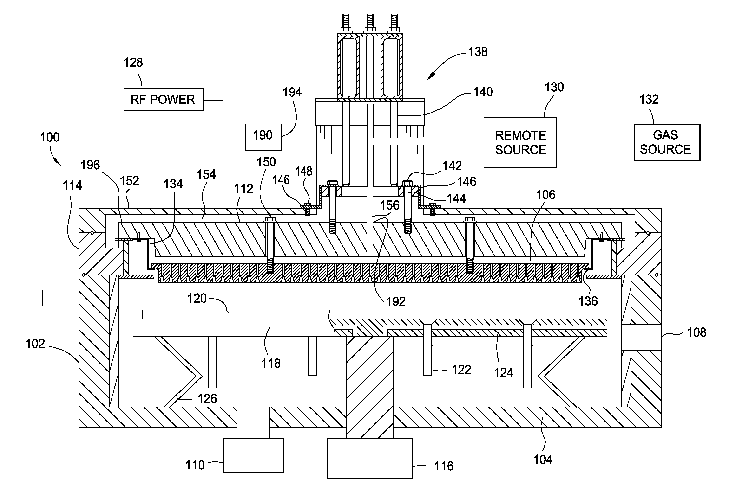
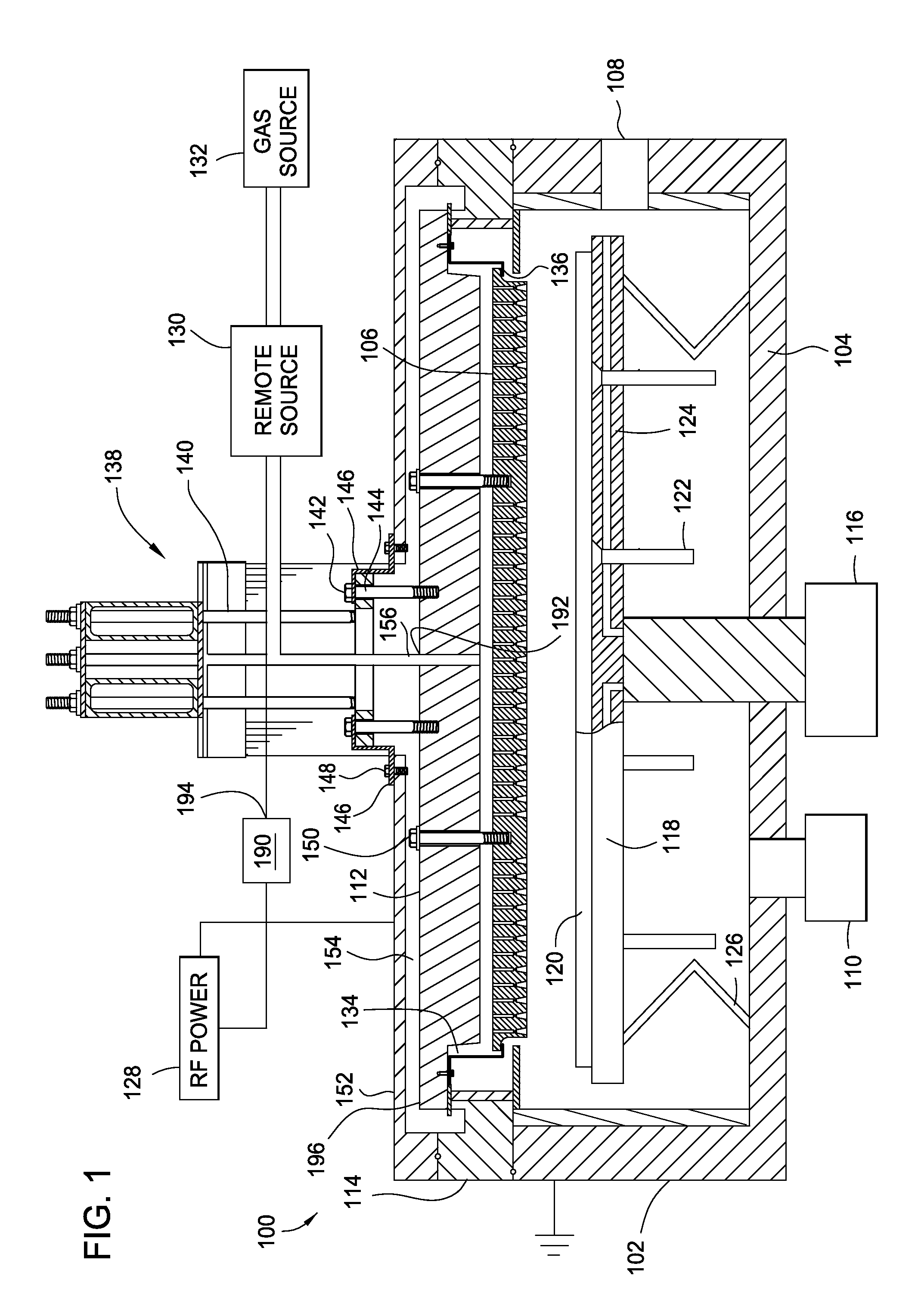
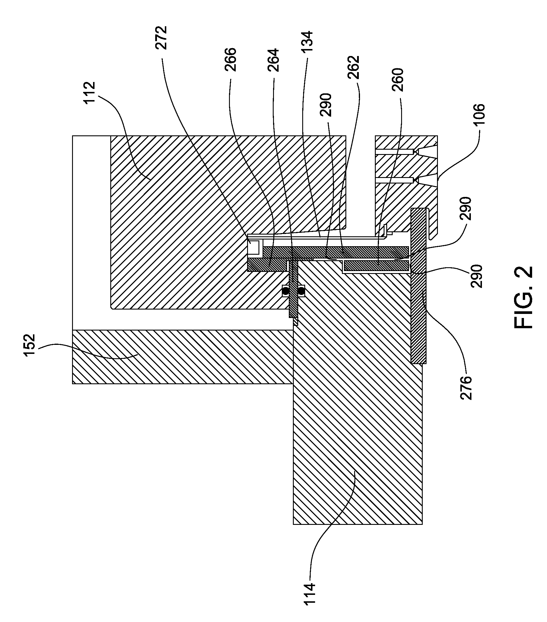
The present invention generally relates to a capacitively coupled plasma (CCP) processing chamber, a manner to reduce or prevent stray capacitance, and a manner to measure plasma conditions within the processing chamber. As CCP processing chambers increase in size, there is a tendency for stray capacitance to negatively impact the process. Additionally, RF ground straps may break. By increasing the spacing between the chamber backing plate and the chamber wall, stray capacitance may be minimized. Additionally, the plasma may be monitored by measuring the conditions of the plasma at the backing plate rather than at the match network. In so measuring, the plasma harmonic data may be analyzed to reveal plasma processing conditions within the chamber.
Need to check novelty before this filing date? Find Prior Art

Description

CROSS-REFERENCE TO RELATED APPLICATIONS

[0001] This application claims benefit of U.S. Provisional Patent Application Ser. No. 61 / 536,760 (APPM / 14722L), filed Sep. 20, 2012, which is herein incorporated by reference.BACKGROUND OF THE INVENTION

[0002] 1. Field of the Invention

[0003] Embodiments of the present invention generally relate to a capacitively coupled plasma (CCP) processing chamber, a manner to reduce or prevent stray capacitance, and a manner to measure plasma conditions within the processing chamber.

[0004] 2. Description of the Related Art

[0005] Most, if not all, computers and televisions manufactured are flat panel displays (FPDs). Some of the FPDs are quite large and almost all FPDs are larger than a semiconductor chip that is used in the modern personal computer. To manufacture the FPDs, large area processing chambers (i.e., processing chambers sized to process substrates having a surface area of greater than about 1600 cm2) are oftentimes utilized rather than the smaller ch...

Examples

Embodiment Construction

[0020]The present invention generally relates to a CCP processing chamber, a manner to reduce or prevent stray capacitance, and a manner to measure plasma conditions within the processing chamber. As CCP processing chambers increase in size, there is a tendency for stray capacitance to negatively impact the process. Additionally, RF ground straps may break. By increasing the spacing between the chamber backing plate and the chamber wall, stray capacitance may be minimized. Additionally, the plasma may be monitored by measuring the conditions of the plasma at the backing plate rather than at the match network. In so measuring, the plasma harmonic data may be analyzed to reveal plasma processing conditions within the chamber.

[0021]Embodiments discussed herein may be practiced in a PECVD chamber available from AKT America, a subsidiary of Applied Materials, Inc., Santa Clara, Calif. It is to be understood that the embodiments discussed herein may be practiced in other processing system...