Method of driving electro-optic device and electro-optic device

a technology of electrooptic devices and pixel circuits, which is applied in the direction of static indicating devices, instruments, etc., can solve the problems of increased transistors and/or capacitors in pixel circuits that cannot be avoided, and may still occur so as to prevent or reduce deterioration of display quality and reduce the number of pixel circuits

Active Publication Date: 2013-05-09
SAMSUNG DISPLAY CO LTD
View PDF4 Cites 26 Cited by
  • Summary
  • Abstract
  • Description
  • Claims
  • Application Information

AI Technical Summary

Benefits of technology

[0014]Exemplary embodiments of the present invention sufficiently obtain a threshold voltage compensation time of a driving transistor and a data writing time while reducing a number of elements of a pixel circuit. In addition, the present invention provides a driving method of an electro-optic device and an electro-optic device in which deterioration of display quality is prevented.
[0017]As a result, the driving method of the electro-optic device according to the present invention sufficiently obtains a threshold voltage compensation time of the driving transistor and the data writing time while reducing the number of pixel circuits, thereby preventing deterioration of the display quality.
[0031]As a result, the threshold voltage compensation time of the driving transistor and the data writing time may be sufficiently obtained while reducing the number of pixel circuits, thereby preventing or reducing deterioration of display quality such that a new and improved driving method of the electro-optic device and the electro-optic device may be provided.

Problems solved by technology

While performing the high-speed driving, it is difficult to obtain sufficient threshold voltage compensation time and data writing time of the driving transistor in the pixel circuit such that deterioration of the display quality may be generated.
To solve these problems, increasing the number of transistors and / or capacitors in the pixel circuit cannot be avoided.
However, in these techniques, the threshold voltage compensation of the driving transistor, and the data writing and reference potential writing of the pixel circuit, are performed during each scan line selection period such that the threshold voltage compensation time of the driving transistor and the data writing time may not be sufficiently obtained, and thereby the deterioration of the display quality may still occur.
Particularly, these problems are more significant when the scan line selection period is short while performing surface sequential driving for the 3-D image display.

Method used


Image

  • Method of driving electro-optic device and electro-optic device
  • Method of driving electro-optic device and electro-optic device
  • Method of driving electro-optic device and electro-optic device

Examples


first exemplary embodiment

1. First Exemplary Embodiment

Constitution of a Pixel Circuit of an Electro-Optic Device

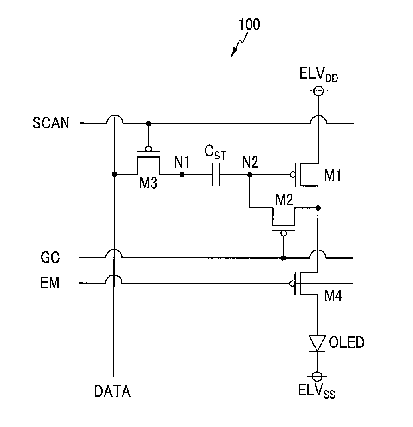
[0053]Firstly, a constitution of a pixel circuit of an electro-optic device according to a first exemplary embodiment of the present invention will be described.

[0054]FIG. 1 is a diagram of a pixel circuit 100 of an electro-optic device according to the first exemplary embodiment of the present invention.

[0055]The electro-optic device according to the first exemplary embodiment of the present invention has a matrix type structure in which the pixel circuit 100 shown in FIG. 1 is disposed at a crossing position of, for example, a scan line of an n-th row and a data line of an m-th column.

[0056]Next, the pixel circuit of the electro-optic device according to the first exemplary embodiment of the present invention will be described with reference to FIG. 1.

[0057]As shown in FIG. 1, the pixel circuit 100 of the electro-optic device according to the first exemplary embodiment of the present invention i...

second exemplary embodiment

2. Second Exemplary Embodiment

Constitution of the Pixel Circuit of the Electro-Optic Device

[0120]Next, a constitution of the pixel circuit of the electro-optic device according to a second exemplary embodiment of the present invention will be described.

[0121]FIG. 5 is a diagram of a pixel circuit 200 of an electro-optic device according to the second exemplary embodiment of the present invention.

[0122]The electro-optic device of a matrix type according to the second exemplary embodiment of the present invention includes the pixel circuit 200 shown in FIG. 5, and the pixel circuit 200 is disposed at a crossing position of, for example, a scan line of an n-th row and a data line of an m-th column.

[0123]Next, the pixel circuit 200 of the electro-optic device according to the second exemplary embodiment of the present invention will be described with reference to FIG. 5.

[0124]As shown in FIG. 5, the pixel circuit 200 of the electro-optic device according to the second exemplary embodime...

third exemplary embodiment

3. Third Exemplary Embodiment

Constitution of the Pixel Circuit of the Electro-Optic Device

[0170]Next, a constitution of a pixel circuit of an electro-optic device according to a third exemplary embodiment of the present invention will be described.

[0171]FIG. 8 is a diagram of a pixel circuit 200 of an electro-optic device according to the third exemplary embodiment of the present invention.

[0172]The electro-optic device of a matrix type according to the third exemplary embodiment of the present invention includes the pixel circuit 300 shown in FIG. 8, and the pixel circuit 300 is disposed at a crossing position of a scan line of, for example, an n-th row and a data line of an m-th column.

[0173]Next, the pixel circuit 300 of the electro-optic device according to the third exemplary embodiment of the present invention will be described with reference to FIG. 8.

[0174]As shown in FIG. 8, the pixel circuit 300 of the electro-optic device according to the third exemplary embodiment of the...


PUM


Abstract

A driving method of an electro-optic device is capable of sufficiently providing a threshold voltage compensation time of a driving transistor and a data writing time. A driving method of an electro-optic device including a first power source, a second power source, data lines, scan lines, signal lines, and pixel circuits, includes: a first step in which a light emitting element is in a non-light-emitting state, and a second transistor is turned on by a change of a pulse applied to a signal line; and a second step in which the scan line is sequentially and exclusively selected after the second transistor is turned on, a third transistor including a gate connected to a selected scan line is turned on, and a corresponding data voltage is written to a first node from the data line through the third transistor.

Description

CROSS-REFERENCE TO RELATED APPLICATION[0001]This application claims priority to and the benefit of Japanese Patent Application No. 2011-245724 filed in the Japan Patent Office on Nov. 9, 2011, the entire contents of which are incorporated herein by reference.BACKGROUND[0002](a) Field[0003]Embodiments of the present invention relate to a driving method of an electro-optic device, and an electro-optic device.[0004](b) Description of the Related Art[0005]As a display unit for a television set, a liquid crystal display (LCD) including a transmissive or transflective liquid crystal panel, or an organic light emitting diode (OLED) display including an organic light emitting diode (OLED) panel consisting of a number of organic light emitting elements, is widely used.[0006]Recently, high-speed driving of a pixel circuit in an electro-optic device has been used in a display of a high resolution or a 3-D image.[0007]While performing the high-speed driving, it is difficult to obtain sufficient...

Claims


Application Information

Patent Timeline
Patent Type & Authority Applications(United States)
IPC IPC(8): G09G3/30
CPCG09G3/003G09G3/3233G09G2300/0861G09G2300/0842G09G2300/0819G09G3/20G09G3/30
Inventor ISHII, RYOKATSUSE, HIROFUMIOKUNO, TAKESHIKOMIYA, NAOAKI
Owner SAMSUNG DISPLAY CO LTD
Why Eureka
Try Eureka