

Wiring substrate and electronic device
a technology of wiring substrate and electronic device, which is applied in the direction of cross-talk/noise/interference reduction, printed circuit details, printed circuits, etc., can solve the problem of not being able to suppress electromagnetic noise leakage, and achieve the effect of suppressing electromagnetic noise leakag
- Summary
- Abstract
- Description
- Claims
- Application Information
AI Technical Summary
Benefits of technology
Problems solved by technology
Method used
Image

Examples
first embodiment
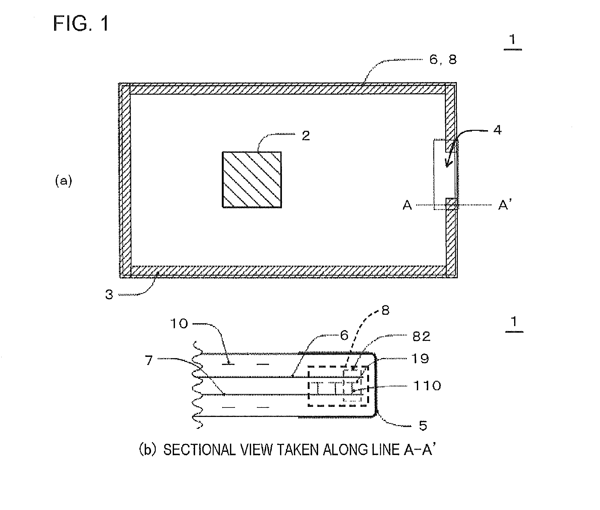
[0025]FIG. 1(a) is a plan view showing the configuration of a wiring substrate 1 according to a first embodiment, and FIG. 1(b) is a sectional view taken along the line A-A′ of FIG. 1(a). The wiring substrate 1 includes a multilayered wiring layer, a structure 8 of a conductor, and an electromagnetic wave absorber 5. An electronic component 2 which is an example of an electromagnetic noise generation source is mounted on the wiring substrate 1. The electronic component 2 has a high-frequency circuit. The structure 8 is formed using the multilayered wiring layer, and is arranged so as to enclose the electronic component 2 in plan view with an opening 4 in the enclosure. The electromagnetic wave absorber 5 is arranged so as to cover the opening 4. Hereinafter, detailed description will be provided.
[0026]The wiring substrate 1 is, for example, a printed wiring substrate, and has a multilayered wiring structure as described above. For example, the wiring substrate 1 has a power layer 6,...
second embodiment
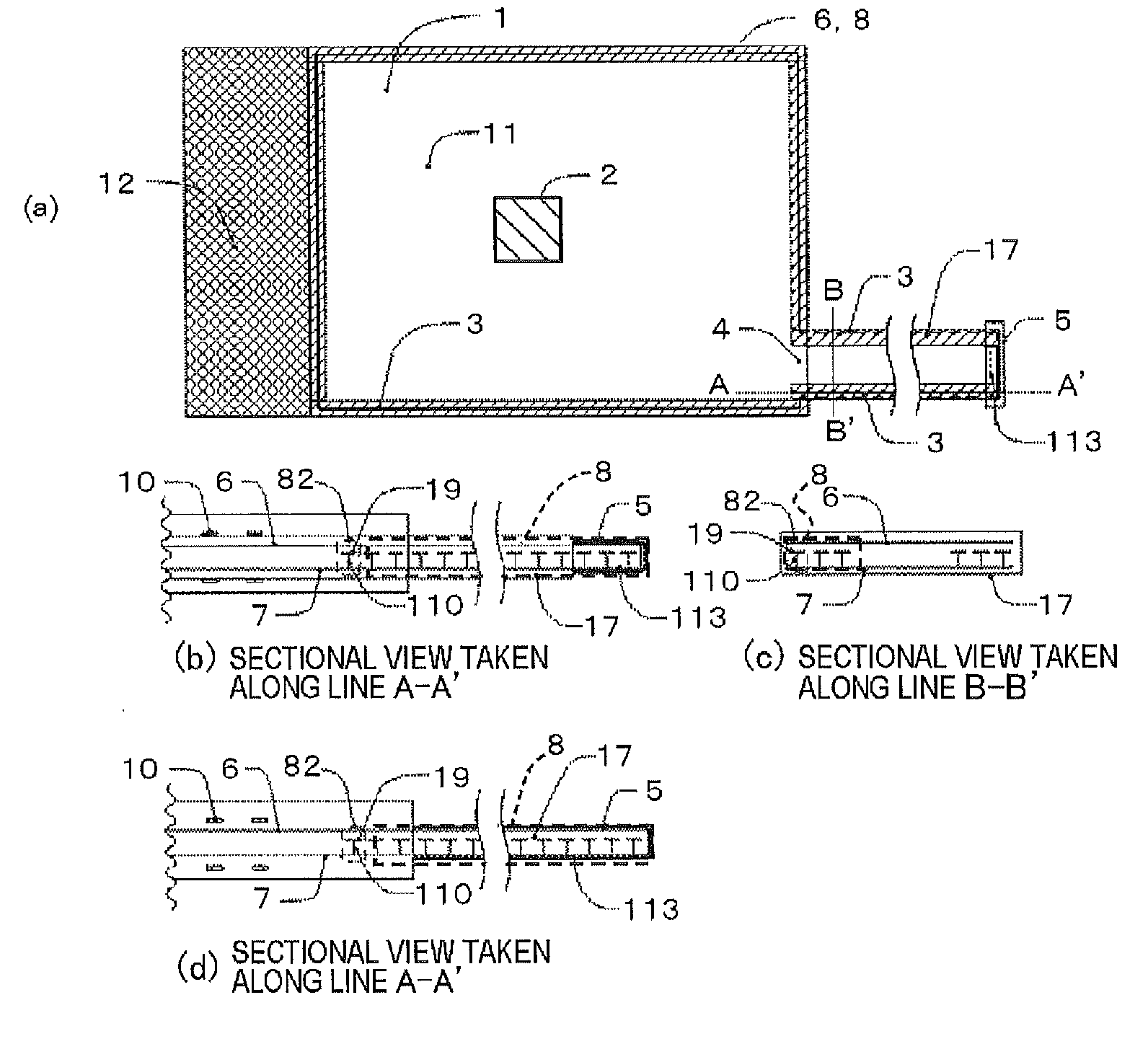
[0039]FIG. 5(a) is a plan view showing the configuration of a wiring substrate according to a second embodiment, and FIG. 5(b) is a sectional view taken along the line A-A′ of FIG. 5(a). A wiring substrate 1 of this embodiment has the same configuration as the wiring substrate 1 of the first embodiment excluding the following points.
[0040]First, the wiring substrate 1 has a first region 11 where a digital circuit is provided, and a second region 12 where an analog circuit is provided. The electronic component 2 which becomes an electromagnetic noise generation source is provided in the first region 11. The structure 8 and the electromagnetic wave absorber 5 are laid out so as to enclose the first region 11 and not to enclose the second region 12.
[0041]The electromagnetic wave absorber 5 has an upper absorber 51 and a lower absorber 52. The upper absorber 51 is pasted from the front surface of the wiring substrate 1 to the center of the lateral surface, and the lower absorber 52 is p...
third embodiment
[0043]FIG. 6(a) is a plan view showing the configuration of a wiring substrate 1 according to a third embodiment, and FIG. 6(b) is a sectional view taken along the line A-A′ of FIG. 6(a). The wiring substrate 1 of this embodiment has the same configuration as the wiring substrate 1 according to the second embodiment excluding that the opening portion 4 and the electromagnetic wave absorber 5 are provided at multiple locations, and a through via (through hole) 111 is provided instead of the via (through hole) 110.
[0044]In the embodiment, the opening portion 4 and the electromagnetic wave absorber 5 are provided at both ends of one short side of the wiring substrate 1. The through via 111 is formed to pass from the upper surface to the rear surface of the wiring substrate 1.
[0045]In this embodiment, the same effects as in the second embodiment can be obtained. Since the opening portion 4 and the electromagnetic wave absorber 5 are provided at multiple locations, electromagnetic noise ...
PUM
 Abstract
Description
Claims
Application Information