

Thin Film Transistor, Fabrication Method Thereof, and Organic Light Emitting Diode Display Having the Same
a technology of thin film transistor and fabrication method, which is applied in the direction of transistors, solid-state devices, thermoelectric devices, etc., can solve the problems of difficult implementation of high-resolution panes and spatial loss, and achieve excellent driving margin, reduce fabrication unit costs, and enhance production efficiency
- Summary
- Abstract
- Description
- Claims
- Application Information
AI Technical Summary
Benefits of technology
Problems solved by technology
Method used
Image

Examples
Embodiment Construction
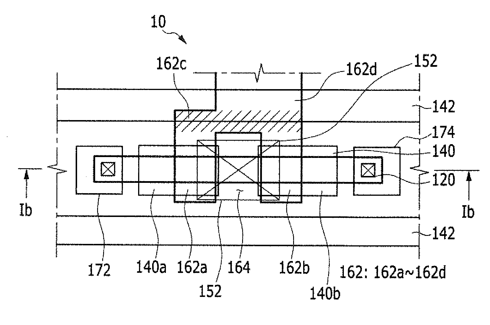
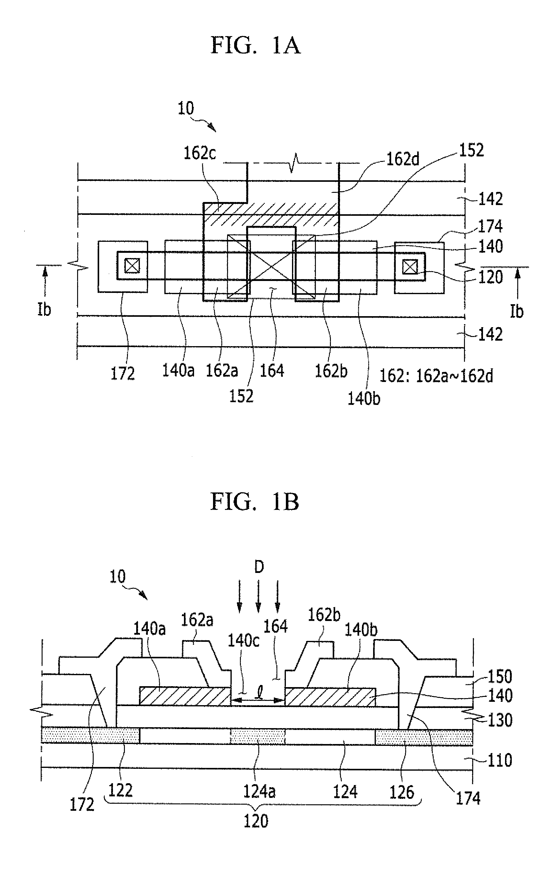
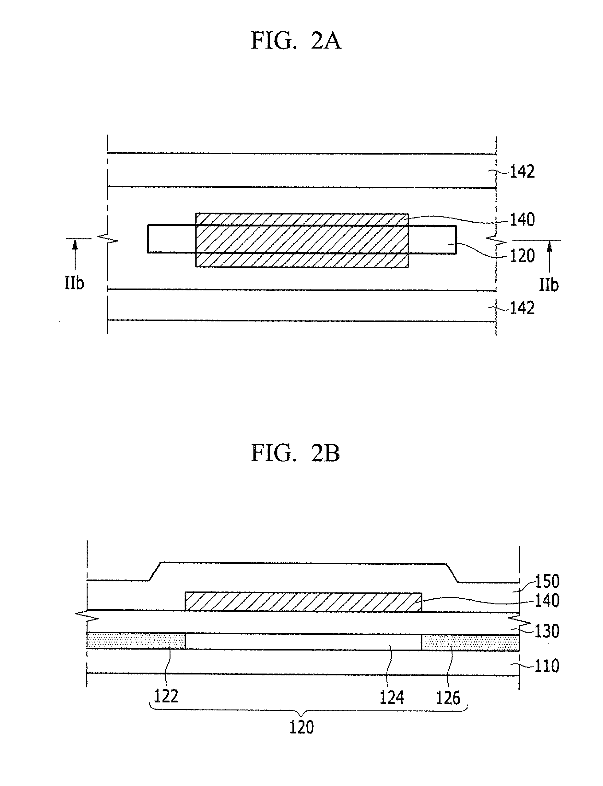
[0025]Hereinafter, a thin film transistor (TFT), a fabrication method thereof, and an organic light emitting diode (OLED) display device having the same will be described in detail with reference to the accompanying drawings. The invention may, however, be embodied in many different forms and should not be construed as being limited to the embodiments set forth herein. Rather, these embodiments are provided so that this disclosure will be thorough and complete, and will fully convey the scope of the invention to those skilled in the art. In the drawings, the same reference numerals will be used throughout to designate the same or like components.
[0026]In the drawings, the thickness of several layers and regions are magnified for clarification, in the drawings, the thickness of some of layers and regions are exaggerated for the sake of explanation. It will be understood that, when an element such as a layer, film, region, or plate is referred to as being “on” another element, it can ...
PUM
 Abstract
Description
Claims
Application Information