Flexible active device array substrate and organic electroluminescent device having the same

a flexible, array substrate technology, applied in the direction of organic semiconductor devices, thermoelectric devices, solid-state devices, etc., can solve the problems of affecting the electrical properties of tft, cracking in the passivation layer after tft, and poor water resistance of organic materials, etc., to achieve favorable reliability

Inactive Publication Date: 2013-05-23
AU OPTRONICS CORP
View PDF6 Cites 16 Cited by
  • Summary
  • Abstract
  • Description
  • Claims
  • Application Information

AI Technical Summary

Benefits of technology

[0008]The application is directed to a flexible active device array substrate and an organic electroluminescent device with favorable reliability.

Problems solved by technology

Nonetheless, in the process of fabricating a flexible organic electroluminescent device, the unfavorable flexibility of the inorganic material may cause cracks in the passivation layer after the TFT is bent.
Thereby, water vapor (humidity) penetrates the passivation layer through the cracks and thus affects the electrical properties of the TFT.
However, water resistance of the organic material is not as good as that of the inorganic material, and accordingly water vapor (humidity) is apt to penetrate the TFT and thereby affects the electrical properties of the TFT.
In comparison with the common rigid substrate (e.g., a glass substrate), when a flexible substrate applied is made of plastic, water vapor (humidity) is prone to penetrate the TFT through a direction of the plastic substrate, thus posing an impact on the electrical properties of the TFT.
As a result, how to improve the reliability of a flexible active device array substrate is one of the issues to be resolved imminently.

Method used


Image

  • Flexible active device array substrate and organic electroluminescent device having the same
  • Flexible active device array substrate and organic electroluminescent device having the same
  • Flexible active device array substrate and organic electroluminescent device having the same

Examples


Embodiment Construction

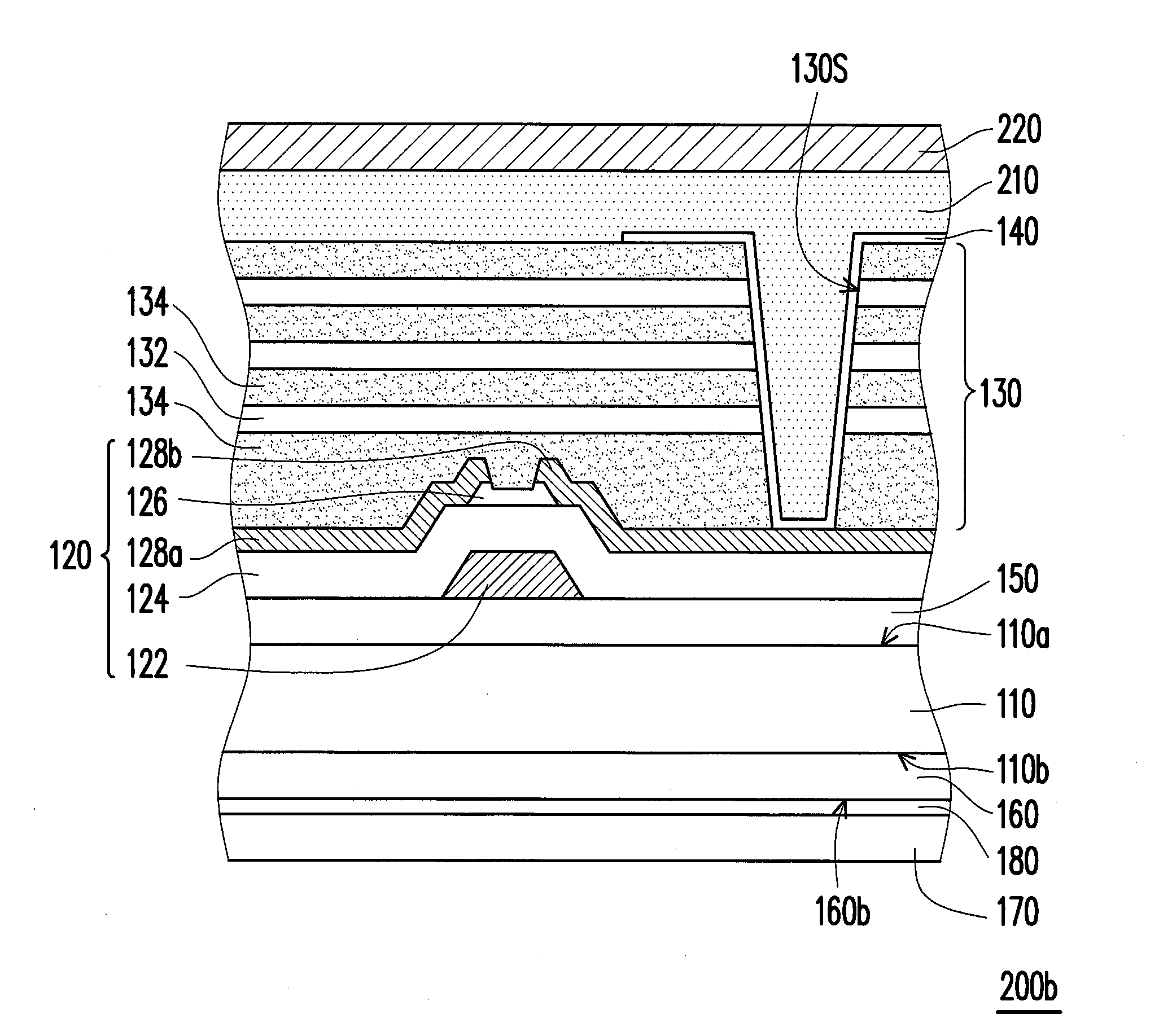
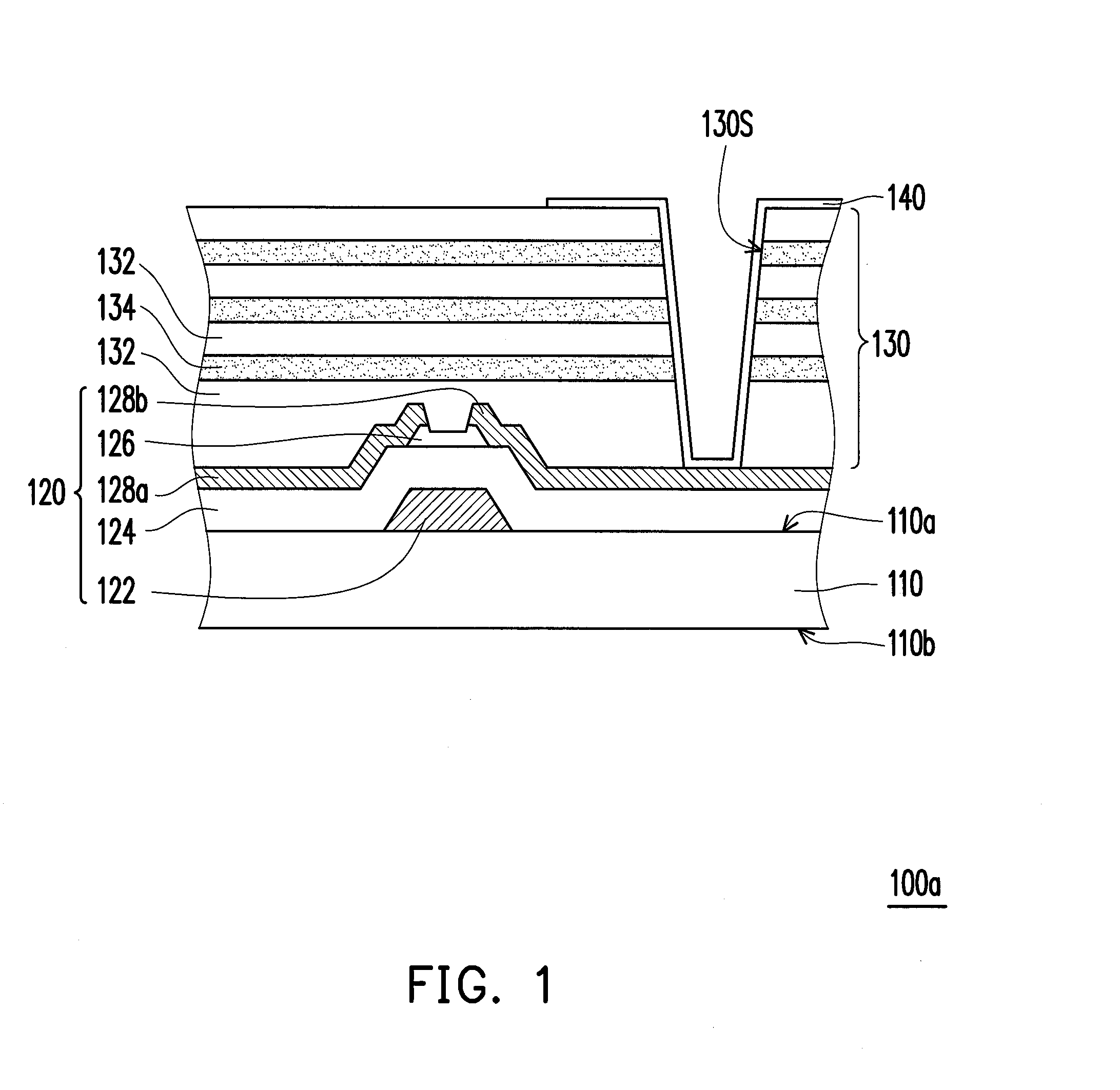
[0030]FIG. 1 is a schematic cross-sectional view illustrating a flexible active device array substrate 100a according to a first embodiment of the invention. With reference to FIG. 1, the flexible active device array substrate 100a includes a flexible substrate 110, an active device array layer 120, a barrier layer 130, and a plurality of pixel electrodes 140 according to the present embodiment. The active device array layer 120 is disposed on the flexible substrate 110. The barrier layer 130 covers the active device array layer 120. The barrier layer 130 includes a plurality of organic material layers 132 and a plurality of inorganic material layers 134. The organic material layers 132 and the inorganic material layers 134 are alternately stacked on the active device array layer 120. The pixel electrodes 140 are disposed on the barrier layer 130, and each of the pixel electrodes 140 is electrically connected to the active device array layer 120.

[0031]The flexible substrate 110 has ...


PUM


Abstract

A flexible active device array substrate including a flexible substrate, an active device array layer, a barrier layer, and a plurality of pixel electrodes is provided. The active device array layer is disposed on the flexible substrate. The barrier layer covers the active device array layer. The barrier layer includes a plurality of organic material layers and a plurality of inorganic material layers. The organic material layers and the inorganic material layers are alternately stacked on the active device array layer. The pixel electrodes are disposed on the barrier layer, and each of the pixel electrodes is electrically connected to the active device array layer.

Description

CROSS-REFERENCE TO RELATED APPLICATION[0001]This application claims the priority benefit of Taiwan application serial no. 100142005, filed on Nov. 17, 2011. The entirety of the above-mentioned patent application is hereby incorporated by reference herein and made a part of this specification.BACKGROUND OF THE INVENTION[0002]1. Field of the Invention[0003]The application relates to an active device array substrate, and in particular to a flexible active device array substrate.[0004]2. Description of Related Art[0005]Organic electroluminescent devices have been considered a dominant flat panel display in the future because of their desirable qualities of compactness, self-luminescence, low power consumption, no need of backlight source, no viewing angle limitation, and high response speed. To be able to broadly apply the organic electroluminescent device, a flexible organic electroluminescent device has been developed. Whether a display is flexible is determined by a material of a sub...

Claims


Application Information

Patent Timeline
Patent Type & Authority Applications(United States)
IPC IPC(8): H01L27/15H01L27/10
CPCH01L51/5253H01L2251/5338H01L27/3258H01L51/5256H10K59/124H10K50/844H10K50/8445H10K2102/311
Inventor CHAN, CHI-SHUNHUNG, SHIH-HSINGHU, CHIH-JEN
Owner AU OPTRONICS CORP
Why Eureka
Try Eureka