
Flash memory

Inactive Publication Date: 2013-06-06
NATIONAL CHIAO TUNG UNIVERSITY
View PDF13 Cites 6 Cited by
  • Summary
  • Abstract
  • Description
  • Claims
  • Application Information

AI Technical Summary

Benefits of technology

The present invention provides a flash memory with a charge-trapping layer formed by implanting arsenic into ZrON, which has improved performance and reliability. The flash memory includes a substrate, layers of SiO2, high-κ layers, and a metal-implanted oxynitride layer with a Ge / oxynitride layer and a second high-κ layer. The method of fabricating the flash memory includes steps of forming layers on the substrate and implanting arsenic into ZrON. The As-implanted ZrON is formed by implanting ZrON with As at 60°-tilted angle, 3 KeV and 5×1015 cm−2 dose, and followed by 950° C. RTA. The technical effect of the invention is that the flash memory has improved performance and reliability.

Problems solved by technology

According to International Technology Roadmap for Semiconductors (ITRS), the degraded endurance and retention are the toughest challenges to further down-scaling the Charge-Trapping Flash (CTF), due to the fewer electrons stored in highly scaled device.
On the other hand, scaling down the Si3N4 charge-trapping layer to 3-4 nm is needed in ITRS for continuous device scaling, but no proposed solution up to now.
However, this worsens the retention and endurance due to the poorer trapping capability at thinner Si3N4, where nearly no charge trapping was found in 2 nm Si3N4.
Such retention and erase-speed trade-off is a basic limitation of CTF.
One drawback of desired higher κ HfON is the lower trapping efficiency; thus, the double trapping HfON—Si3N4 CTF was used.

Method used


Image

  • Flash memory
  • Flash memory
  • Flash memory

Examples


Embodiment Construction

[0028]The following illustrative embodiments are provided to illustrate the disclosure of the present invention, these and other advantages and effects can be apparently understood by those in the art after reading the disclosure of this specification. The present invention can also be performed or applied by other different embodiments. The details of the specification may be on the basis of different points and applications, and numerous modifications and variations can be devised without departing from the spirit of the present invention.

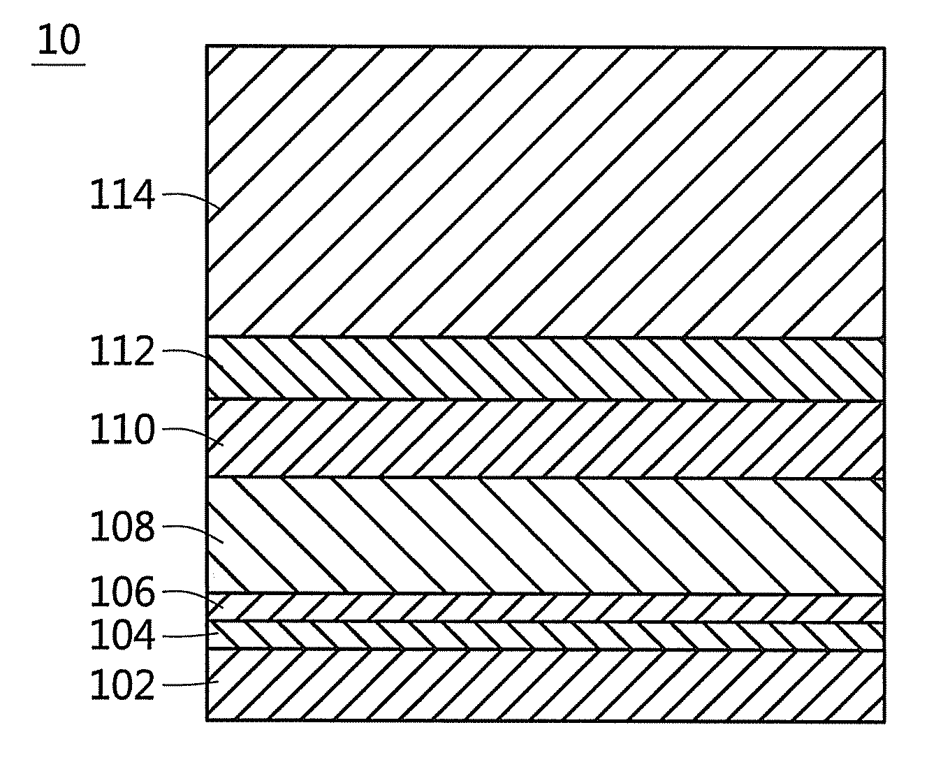
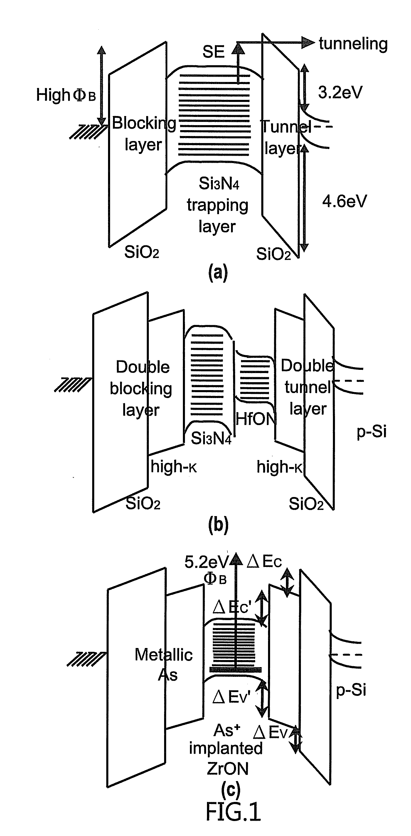
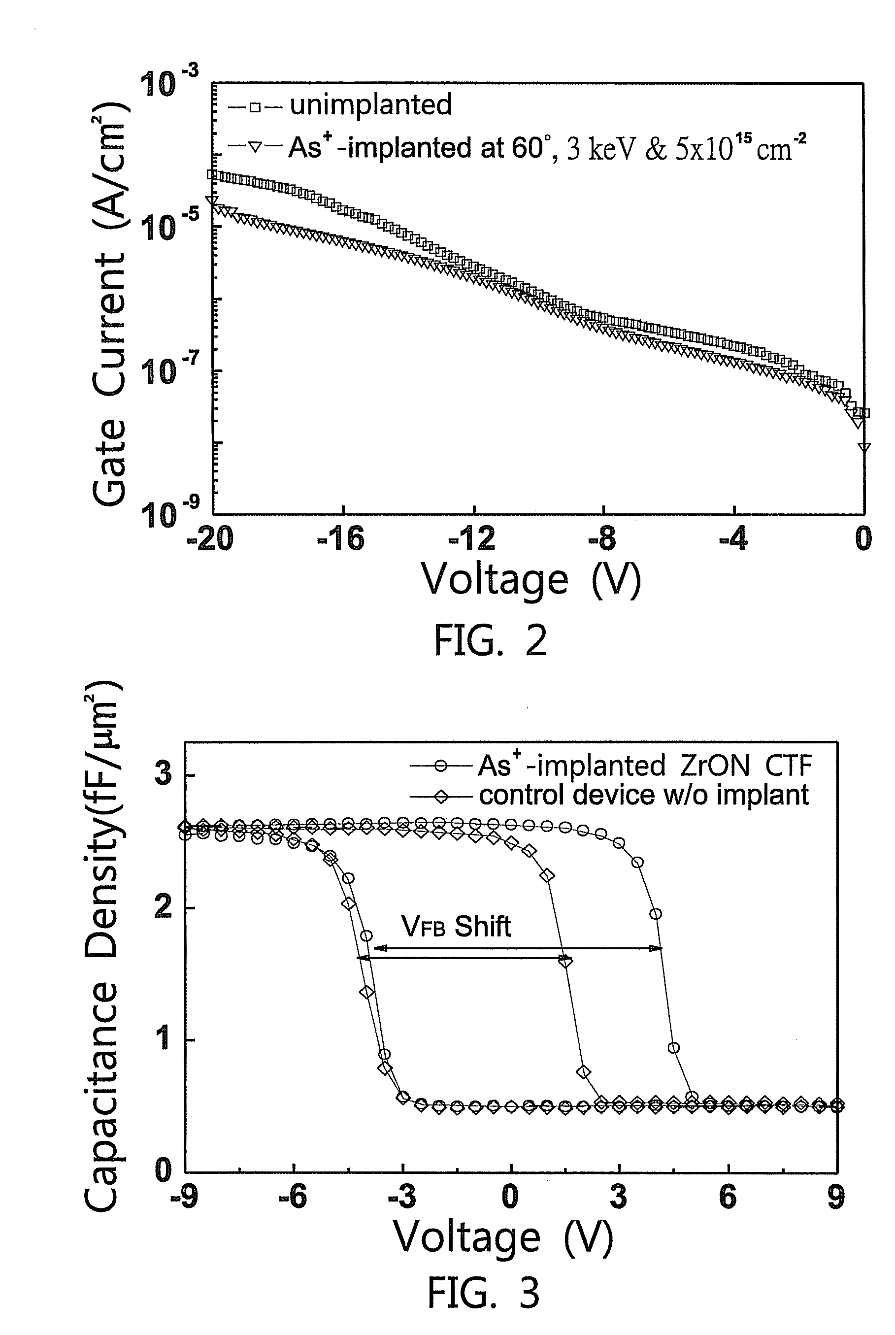
[0029]High performance MONOS CTF with highly scaled 3.6 nm ENT is reached and meets ITRS scaling target for the first time. At 125° C. and ±16 V program / erase (P / E), the device has fast 100 μs speed and large extrapolated 10-year retention of 3.1 V. The excellent results were reached using metallic Arsenic (As) implant into higher κ ZrON (κ=35) as trapping layer. In contrast, small 10-year retention window of 1.9 V is found in control ZrON CTF. T...


PUM


Abstract

A MONOS Charge-Trapping flash (CTF), with record thinnest 3.6 nm ENT trapping layer, has a large 3.1V 10-year extrapolated retention window at 125° C. and excellent 106 endurance at a fast 100 is and ±16 V program / erase. This is achieved using As+-implanted higher κ trapping layer with deep 5.1 eV work-function of As. In contrast, the un-implanted device only has a small 10-year retention window of 1.9 V at 125° C. A MoN—[SiO2—LaAlO3]—[Ge—HfON]—[LaAlO3—SiO2]—Si CTF device is also provided with record-thinnest 2.5-nm Equivalent-Si3N4-Thickness (ENT) trapping layer, large 4.4 V initial memory window, 3.2 V 10-year extrapolated retention window at 125° C., and 3.6 V endurance window at 106 cycles, under very fast 100 μs and low ±16 V program / erase. These were achieved using Ge reaction with HfON trapping layer for better charge-trapping and retention.

Description

BACKGROUND OF THE INVENTION[0001]1. Field of the Invention[0002]This invention relates to flash memories, and, more particularly, to a flash memory having a charge-trapping layer formed by implanting arsenic into ZrON.[0003]2. Description of Related Art[0004]According to International Technology Roadmap for Semiconductors (ITRS), the degraded endurance and retention are the toughest challenges to further down-scaling the Charge-Trapping Flash (CTF), due to the fewer electrons stored in highly scaled device. On the other hand, scaling down the Si3N4 charge-trapping layer to 3-4 nm is needed in ITRS for continuous device scaling, but no proposed solution up to now. However, this worsens the retention and endurance due to the poorer trapping capability at thinner Si3N4, where nearly no charge trapping was found in 2 nm Si3N4. Although the retention is improved by using a thicker tunnel oxide, this yields reduced erase speed. Such retention and erase-speed trade-off is a basic limitatio...

Claims


Application Information

Patent Timeline
IPC IPC(8): H01L29/792H01L21/336
CPCH01L21/28282H01L29/4234H01L29/513H01L29/4966H01L29/66833H01L29/792H01L29/518H01L29/40117
Inventor CHIN, ALBERTTSAI, CHUN-YANG
Owner NATIONAL CHIAO TUNG UNIVERSITY
Features
  • Generate Ideas
  • Intellectual Property
  • Life Sciences
  • Materials
  • Tech Scout
  • Unparalleled Data Quality
  • Higher Quality Content
  • 60% Fewer Hallucinations
Learn More