Crosspoint resistor memory device with back-to-back Schottky diodes

a cross-point resistor and memory device technology, applied in the direction of semiconductor devices, electrical equipment, basic electric elements, etc., can solve the problems of many conventional cross-point resistor memory arrays suffering from read disturbance problems

Inactive Publication Date: 2007-01-18
SHARP LAB OF AMERICA INC
View PDF5 Cites 170 Cited by
  • Summary
  • Abstract
  • Description
  • Claims
  • Application Information

AI Technical Summary

Benefits of technology

[0012] Described herein is a back-to-back diode device that permits current flow in both forward and reverse directions under higher voltage (forward and reverse) bias conditions, but blocks current in under lower voltage bi

Problems solved by technology

Many conventional cross-point resistor memory arrays suffer from read disturbance problems, as electric current flows from a sel

Method used


Image

  • Crosspoint resistor memory device with back-to-back Schottky diodes
  • Crosspoint resistor memory device with back-to-back Schottky diodes
  • Crosspoint resistor memory device with back-to-back Schottky diodes

Examples


Embodiment Construction

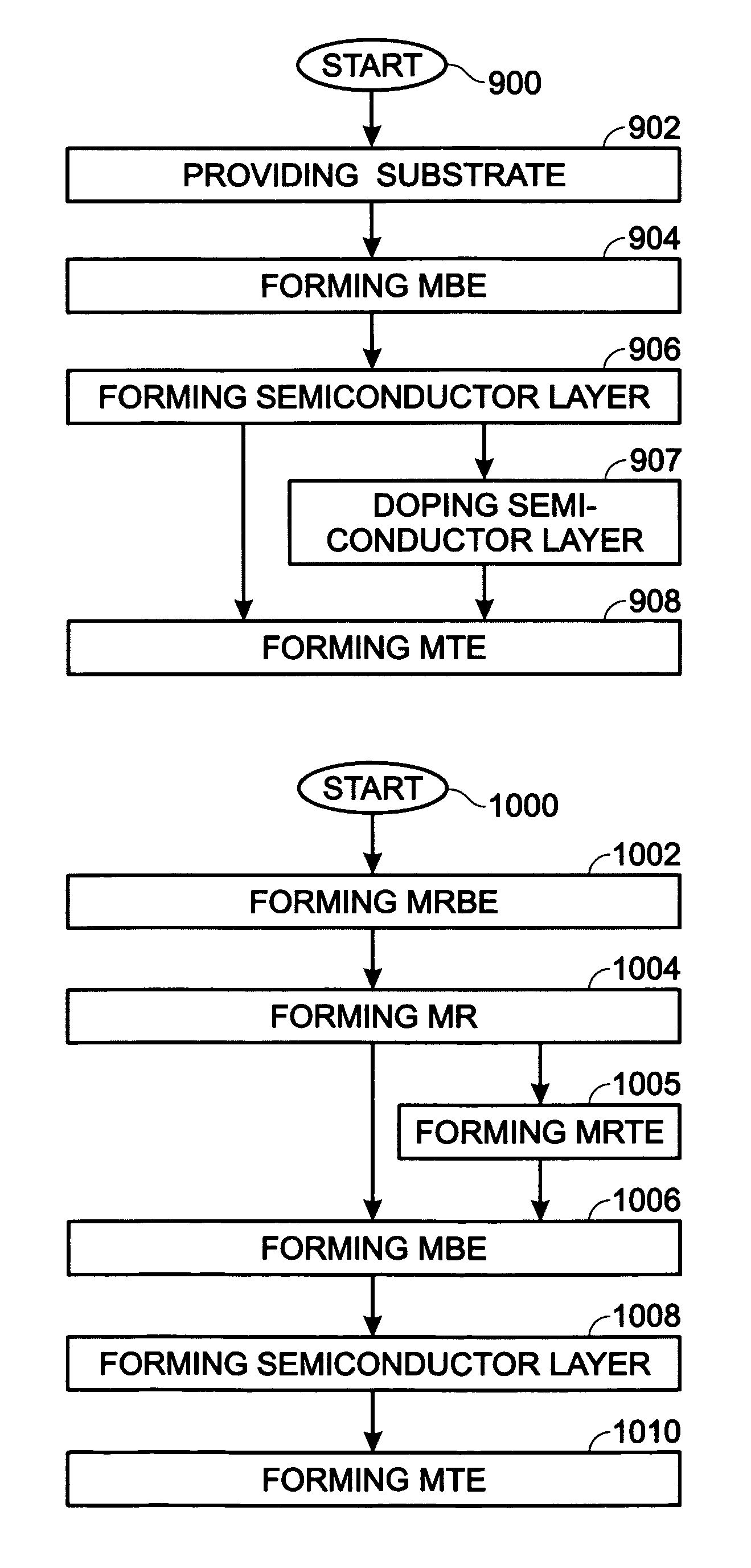
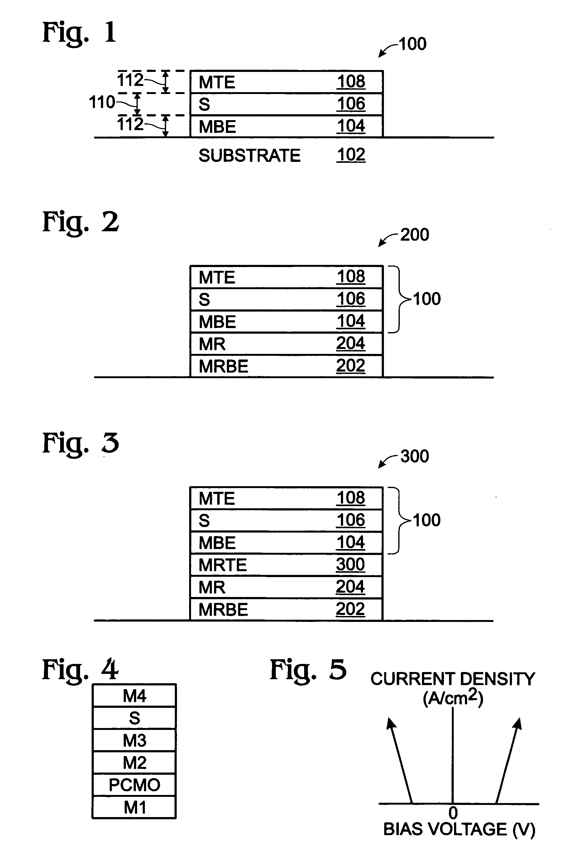
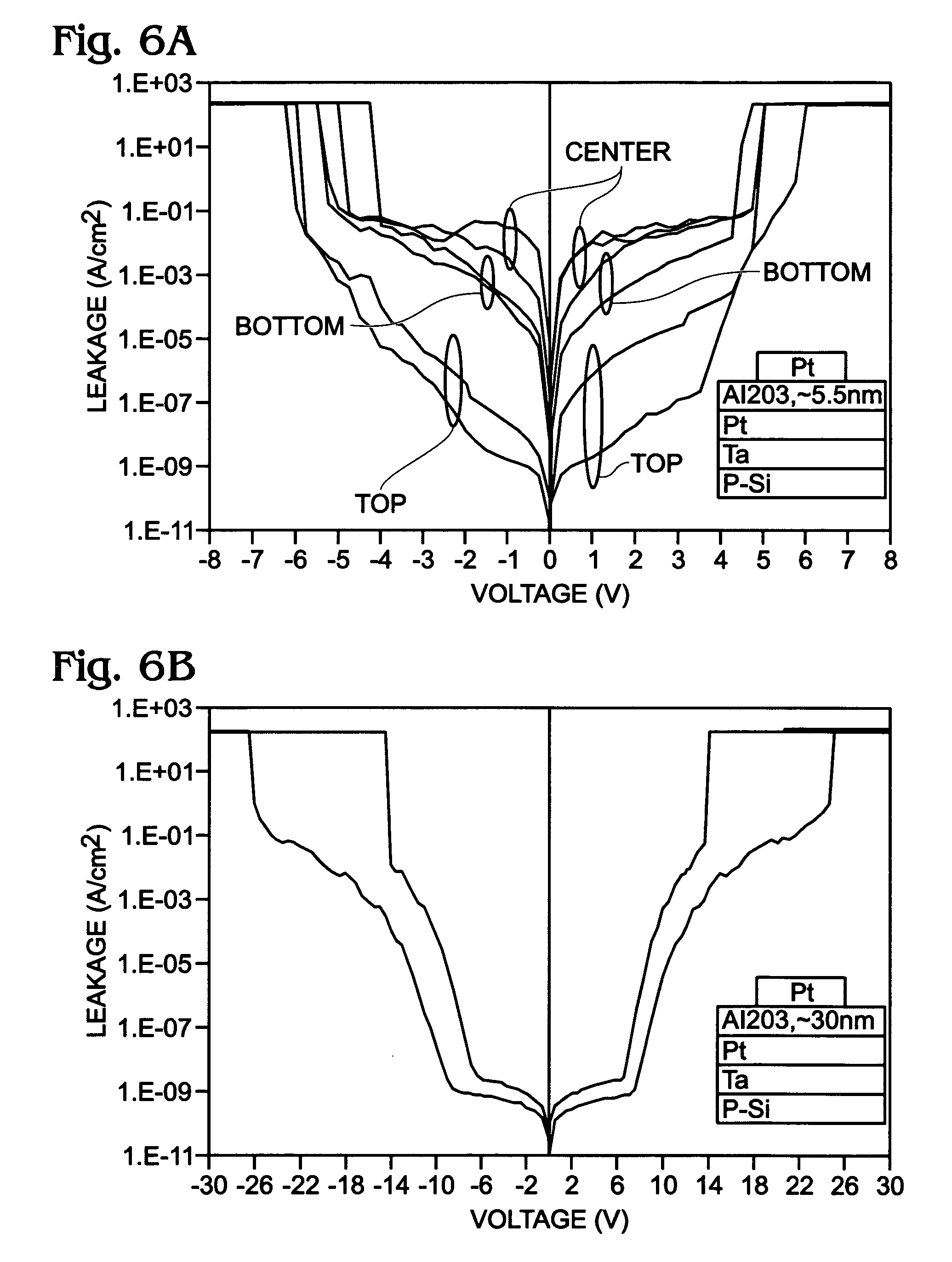
[0028]FIG. 1 is a partial cross-sectional view of a metal / semiconductor / metal (MSM) back-to-back Schottky diode. The MSM diode 100 comprises a substrate 102 and a metal bottom electrode (MBE) 104 overlying the substrate 102. The substrate 102 is not limited to any particular material, and may be a material such as Si, Ge, SiO2, GeAs, glass, quartz, or plastic. The metal bottom electrode 104 has a first work function. A semiconductor layer (S) 106 overlies the metal bottom electrode 104, and has a second work function that is less than the first work function. A metal top electrode 108 overlies the semiconductor layer 106, and has a third work function, greater than the second work function.

[0029] Work function is a measue of the minimum energy, as expressed in electron volts (eV), needed to remove an electron from the Fermi level in a metal, to a far point. Typically, a metal's work function is approximately half the ionization energy of a free atom of the metal. Work function is a...


PUM


Abstract

A metal/semiconductor/metal (MSM) back-to-back Schottky diode, a resistance memory device using the MSM diode, and associated fabrication processes are provided. The method includes: providing a substrate; forming a metal bottom electrode overlying the substrate, having a first work function; forming a semiconductor layer overlying the metal bottom electrode, having a second work function, less than the first work function; and, forming a metal top electrode overlying the semiconductor layer, having a third work function, greater than the second work function. The metal top and bottom electrodes can be materials such as Pt, Au, Ag, TiN, Ta, Ru, or TaN. In one aspect, the metal top electrode and metal bottom electrode are made from the same material and, therefore, have identical work functions. The semiconductor layer can be a material such as amorphous silicon (a:Si), polycrystalline Si, InOx, or ZnO.

Description

RELATED APPLICATIONS [0001] This application is a Continuation-in-Part of a pending patent application entitled, MSM BINARY SWITCH MEMORY DEVICE, invented by Sheng Teng Hsu et al., Ser. No. 11 / 184,660, filed Jul. 18, 2005. [0002] This application is a Continuation-in-Part of a pending patent application entitled, METAL / ZnOx / METAL CURRENT LIMITER, invented by Tingkai Li et al., Ser. No. 11 / 216,398, filed Aug. 31, 2005. [0003] The above-mentioned applications are both expressly incorporated herein by reference, and both claim priority under 35 U.S.C. §120.BACKGROUND OF THE INVENTION [0004] 1. Field of the Invention [0005] This invention generally relates to an integrated circuit (IC) fabrication process and, more particularly, to a crosspoint resistor memory with an MSM device that acts as a back-to-back Schottky diode. [0006] 2. Description of the Related Art [0007] A cross-point memory array is a matrix of memory elements, with electrical contacts arranged along x-axes (i.e., word l...

Claims


Application Information

Patent Timeline
IPC IPC(8): H01L21/28H01L21/44
CPCH01L27/101H01L29/872H01L27/2409H01L45/1233H01L45/147H01L45/04H10B63/20H10N70/20H10N70/826H10N70/8836
Inventor HSU, SHENG TENGLI, TINGKAI
Owner SHARP LAB OF AMERICA INC
Why Eureka
Try Eureka