Replacement Metal Gate Structures Providing Independent Control On Work Function and Gate Leakage Current

a technology of metal gate structure and work function, applied in the field of semiconductor devices, can solve the problems of limiting the performance of conventional semiconductor oxide based gate electrodes, difficult manufacturing of dual metal gate cmos structures, and even more difficult integration of dual gate cmos structures with a replacement gate structur

Inactive Publication Date: 2012-05-31
GLOBALFOUNDRIES INC
View PDF3 Cites 162 Cited by
  • Summary
  • Abstract
  • Description
  • Claims
  • Application Information

AI Technical Summary

Benefits of technology

[0005]The thickness and composition of a gate dielectric can be selected for different types of field effect transistors. A first field effect transistor includes a first gate dielectric having a first U-shaped gate dielectric portion, and a second field effect transistor includes a second gate dielectric having a stack of a planar high dielectric constant material portion and a second U-shaped gate dielectric portion. The planar high dielectric constant material portion can be provided by depositing and patterning a high dielectric constant material layer prior to formation of temporary gate structures. Transistors having different leakage current through a gate dielectric can be formed by selecting whether a planar high dielectric constant portion is present or not.
[0006]Further, the work function of field effect transistors can be tuned independent of selection of the material stack for the gate dielectric. A stack of a barrier metal layer and a first-type work function metal layer having a first-type work function is deposited on a gate dielectric layer within recessed gate cavities after removal of disposable gate material portions. The first-type work function metal layer is patterned to be present in regions of a first type field effect transistor, which can be p-type or n-type transistors, while removed in regions of a second type field effect transistor. A second-type work function metal layer is de

Problems solved by technology

High gate leakage current of silicon oxide and nitrided silicon dioxide as well as depletion effect of polysilicon gate electrodes limits the performance of conventional semiconductor oxide based gate electrodes.
Manufacture of dual metal gate CMOS structures is difficult because two types of metal gate electrodes are needed to provide different work functions.
I

Method used


Image

  • Replacement Metal Gate Structures Providing Independent Control On Work Function and Gate Leakage Current
  • Replacement Metal Gate Structures Providing Independent Control On Work Function and Gate Leakage Current
  • Replacement Metal Gate Structures Providing Independent Control On Work Function and Gate Leakage Current

Examples


first embodiment

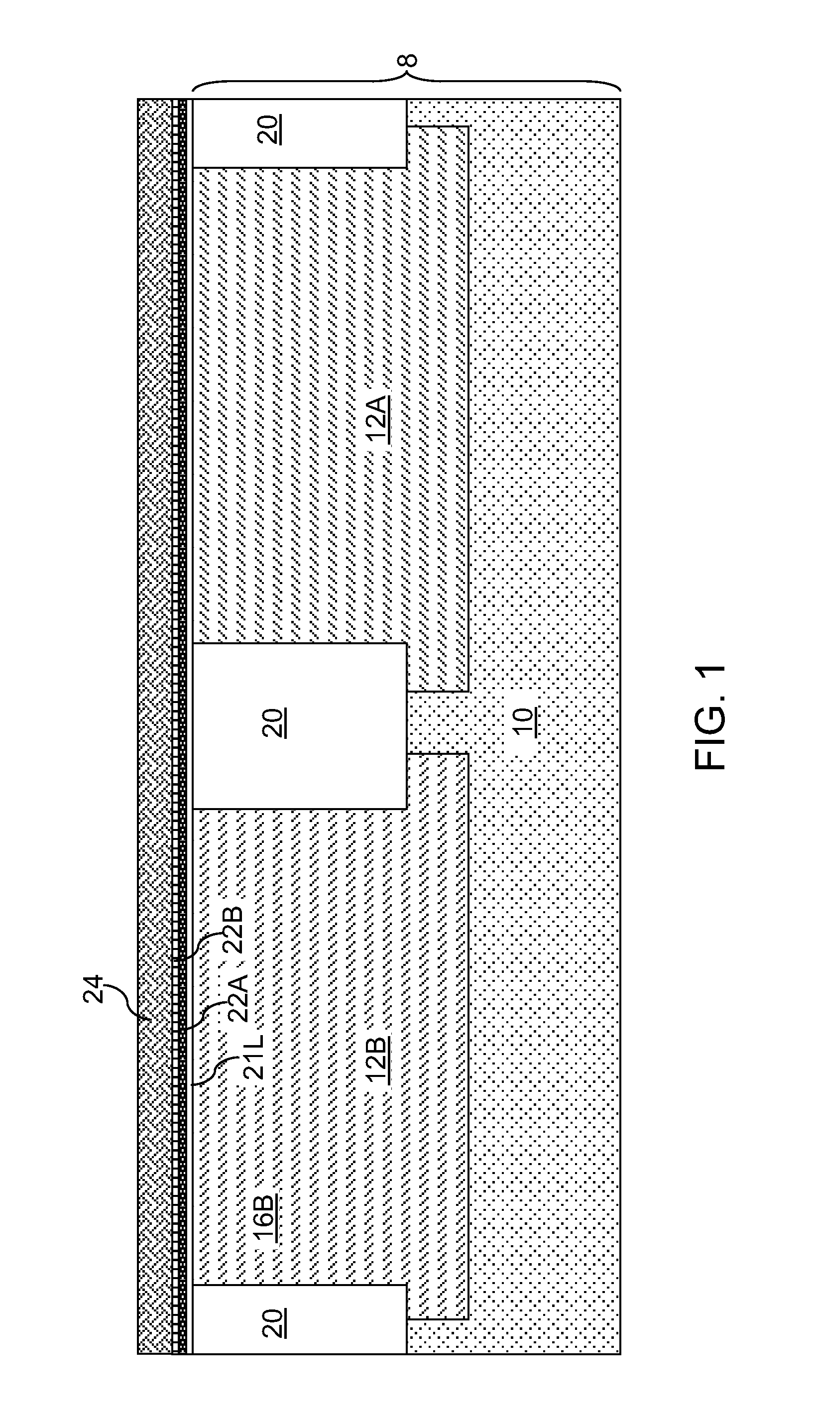
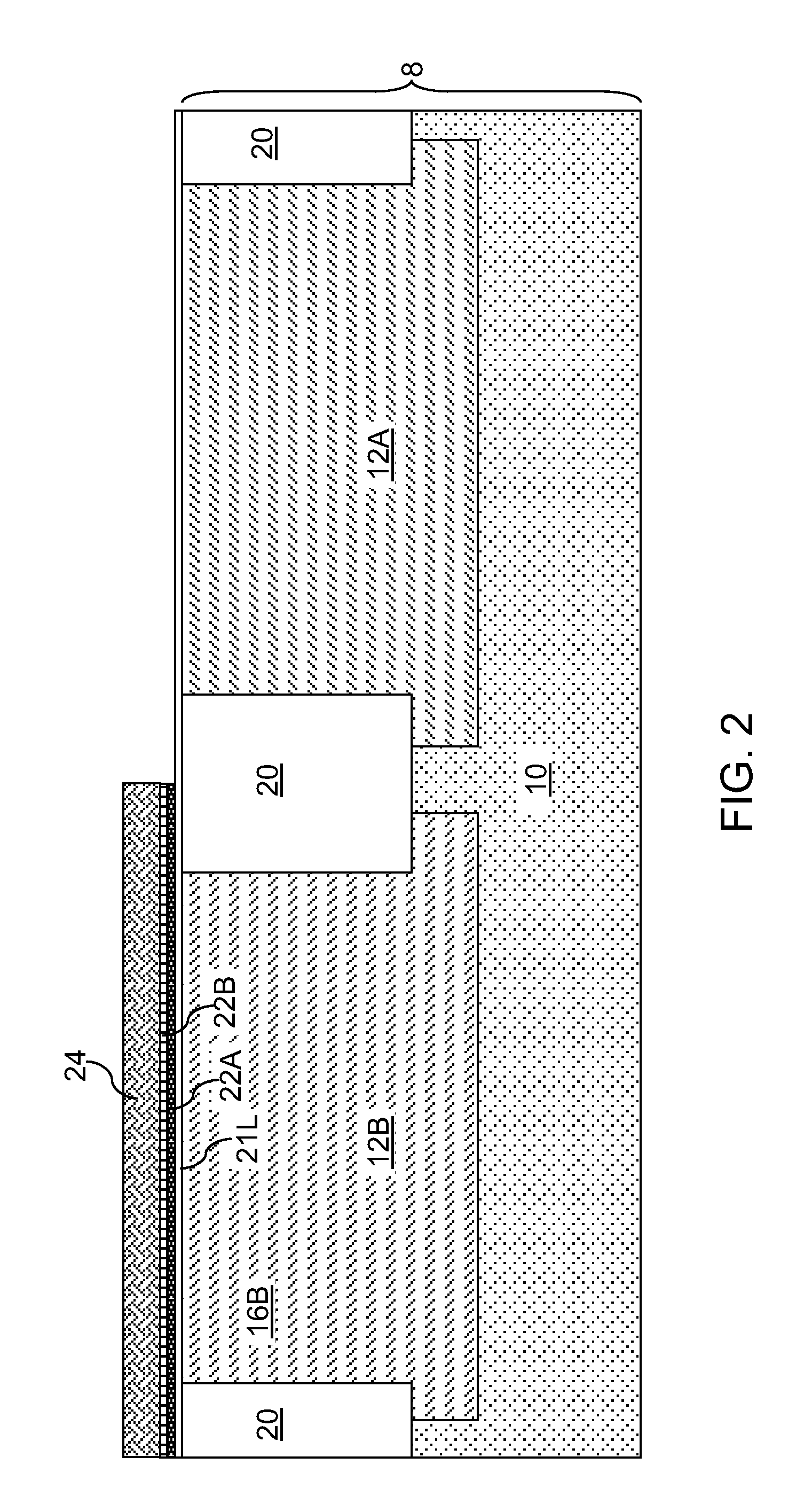
[0028]Referring to FIG. 1, a first exemplary semiconductor structure according to the present disclosure includes a semiconductor substrate 8, on which various components of field effect transistors can be formed. The semiconductor substrate 8 can be a bulk substrate including a bulk semiconductor material throughout, or a semiconductor-on-insulator (SOI) substrate (not shown) containing a top semiconductor layer, a buried insulator layer located under the top semiconductor layer, and a bottom semiconductor layer located under the buried insulator layer. The semiconductor material of the semiconductor substrate 8 may be selected from, but is not limited to, silicon, germanium, silicon-germanium alloy, silicon carbon alloy, silicon-germanium-carbon alloy, gallium arsenide, indium arsenide, indium phosphide, III-V compound semiconductor materials, II-VI compound semiconductor materials, organic semiconductor materials, and other compound semiconductor materials. Typically, the semicon...

third embodiment

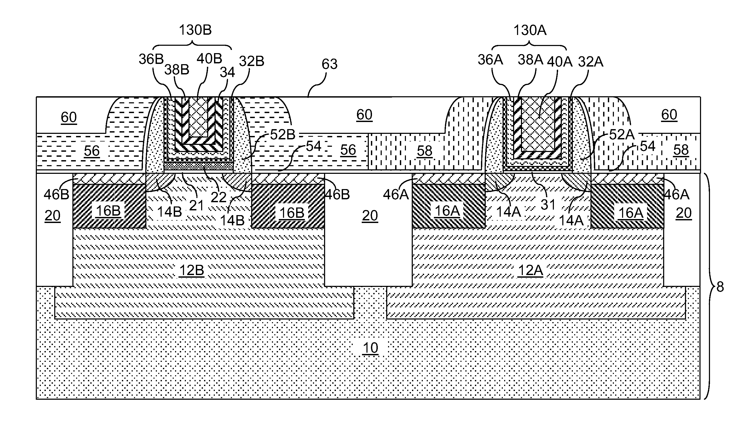
[0105]Further, while the present invention is described employing CMOS field effect transistors as illustrative example, it is understood that the various transistors illustrated in FIGS. 14 and 18 can be formed as a pair of p-type field effect transistors having different work functions or a pair of n-type field effect transistors having different work functions. Each of the four types of field effect transistors in the third embodiment can be formed for p-type field effect transistors or n-type field effect transistors. Thus, a total of eight types of field effect transistors including four p-type field effect transistors and four n-type field effect transistors can be formed on a same semiconductor substrate to provide a wide range of gate leakage current and work functions for p-type field effect transistors and n-type field effect transistors.


PUM


Abstract

The thickness and composition of a gate dielectric can be selected for different types of field effect transistors through a planar high dielectric constant material portion, which can be provided only for selected types of field effect transistors. Further, the work function of field effect transistors can be tuned independent of selection of the material stack for the gate dielectric. A stack of a barrier metal layer and a first-type work function metal layer is deposited on a gate dielectric layer within recessed gate cavities after removal of disposable gate material portions. After patterning the first-type work function metal layer, a second-type work function metal layer is deposited directly on the barrier metal layer in the regions of the second type field effect transistor. A conductive material fills the gate cavities, and a subsequent planarization process forms dual work function metal gate structures.

Description

BACKGROUND[0001]The present disclosure generally relates to semiconductor devices, and particularly to complementary metal-oxide-semiconductor (CMOS) field effect transistors having dual work function metal gates and high-k gate dielectrics having different composition and thickness, and methods of manufacturing the same.[0002]High gate leakage current of silicon oxide and nitrided silicon dioxide as well as depletion effect of polysilicon gate electrodes limits the performance of conventional semiconductor oxide based gate electrodes. High performance devices for an equivalent oxide thickness (EOT) less than 1 nm require high dielectric constant (high-k) gate dielectrics and metal gate electrodes to limit the gate leakage current and provide high on-currents. Materials for high-k gate dielectrics include ZrO2, HfO2, other dielectric metal oxides, alloys thereof, and their silicate alloys.[0003]In general, dual metal gate CMOS integration schemes employ two gate materials, one havin...

Claims


Application Information

Patent Timeline
IPC IPC(8): H01L27/092H01L21/336
CPCH01L21/28088H01L21/82345H01L21/823462H01L21/823842H01L21/823857H01L29/49H01L27/0922H01L29/66545H01L29/7833H01L29/7843H01L27/092H01L27/088H01L29/513
Inventor KWON, UNOHDIVAKARUNI, RAMACHANDRAKRISHNAN, SIDDARTH A.RAMACHANDRAN, RAVIKUMAR
Owner GLOBALFOUNDRIES INC
Why Eureka
Try Eureka