InA1N/GaN heterojunction enhancement type high electron mobility transistor structure and production method thereof

A high electron mobility, enhanced technology, applied in the field of microelectronics, can solve the problems of enhanced device injection damage, depletion effect stability to be verified, etc., to achieve increased operating voltage range, high forward threshold voltage, reduced Effect of Small Gate Leakage Current

Inactive Publication Date: 2008-08-20
XIDIAN UNIV
View PDF0 Cites 34 Cited by
  • Summary
  • Abstract
  • Description
  • Claims
  • Application Information

AI Technical Summary

Problems solved by technology

This method of manufacturing enhanced devices is prone to implantation damage during the ion implantation process, and the dep

Method used


Image

  • InA1N/GaN heterojunction enhancement type high electron mobility transistor structure and production method thereof
  • InA1N/GaN heterojunction enhancement type high electron mobility transistor structure and production method thereof
  • InA1N/GaN heterojunction enhancement type high electron mobility transistor structure and production method thereof

Examples


example 1

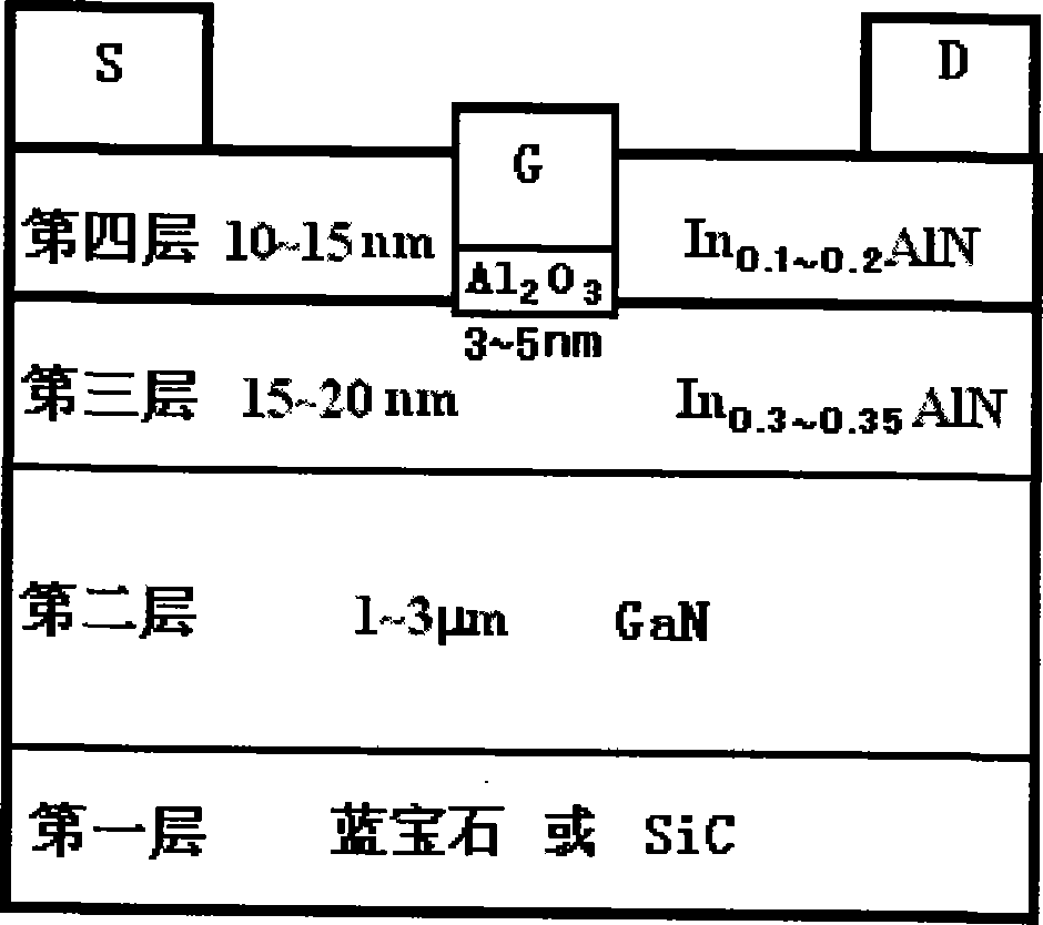
[0039] 1. Epitaxial growth heterojunction materials

[0040] The first step is to grow a GaN buffer layer.

[0041] Use single crystal sapphire as the substrate material to grow the GaN buffer layer in the (0001) direction, that is, first NH at 950℃ 3 And H 2 The sapphire substrate was pretreated at high temperature for 10 minutes in the mixed gas, and then a 30nm low-temperature nucleation layer was grown at 520°C, and then the temperature was raised to 920°C to grow a 1μm thick GaN buffer layer.

[0042] In the second step, the first InAlN layer is epitaxially grown on the GaN layer.

[0043] After the growth of the 1 μm thick GaN buffer layer is completed, the temperature is set to 800° C., and the first InAlN layer with an In composition of 30% is continuously grown, and the thickness of the first InAlN layer is 20 nm.

[0044] In the third step, a second InAlN layer is epitaxially grown on the first InAlN layer.

[0045] After the epitaxial growth on the first InAlN layer is ...

example 2

[0061] 1. Epitaxial growth heterojunction materials

[0062] The first step is to grow a GaN buffer layer.

[0063] Choose a 4H SiC substrate to grow a GaN buffer layer on the Si surface, that is, first NH at 950℃ 3 And H 2 The sapphire substrate was pretreated at high temperature for 10 minutes in the mixed gas, and then a 30nm low-temperature nucleation layer was grown at 520°C, and then heated to 920°C to grow a 2μm thick GaN buffer layer.

[0064] In the second step, the first InAlN layer is epitaxially grown on the GaN layer.

[0065] After the growth of the 2 μm thick GaN buffer layer is completed, the temperature is set to 800° C., and the first InAlN layer with an In composition of 33% is continuously grown, and the thickness of the first InAlN layer is 18 nm.

[0066] In the third step, a second InAlN layer is epitaxially grown on the first InAlN layer.

[0067] After the epitaxial growth on the first InAlN layer is completed, a temperature of 800° C. is set, and a second...

example 3

[0083] 1. Epitaxial growth heterojunction materials

[0084] The first step is to grow a GaN buffer layer.

[0085] Choose a 4H SiC substrate to grow a GaN buffer layer on the Si surface, that is, first NH at 950℃ 3 And H 2 The sapphire substrate was pretreated at high temperature for 10 minutes in the mixed gas, and then a 30nm low-temperature nucleation layer was grown at 520°C, and then the temperature was raised to 920°C to grow a 3μm thick GaN buffer layer.

[0086] In the second step, the first InAlN layer is epitaxially grown on the GaN layer.

[0087] After the growth of the 3 μm thick GaN buffer layer is completed, the temperature is set to 800° C., and the first InAlN layer with an In composition of 35% is continuously grown, and the thickness of the first InAlN layer is 15 nm.

[0088] In the third step, a second InAlN layer is epitaxially grown on the first InAlN layer.

[0089] After the epitaxial growth on the first InAlN layer is completed, a temperature of 800° C. ...


PUM

PropertyMeasurementUnit
Thicknessaaaaaaaaaa
Layer thicknessaaaaaaaaaa
Thicknessaaaaaaaaaa

Abstract

The present invention discloses an InAIN/GaN heterojunction enhanced high electron mobility transistor structure and fabricating method thereof. The steps of manufacture are: 1) epitaxial growth of 1-3 mum GaN on sapphire or SiC substrate; 2) epitaxial growth of 15-20 nm first InAlN layer on GaN, In components is 30-35%, the temperature of epitaxial growth is 800 degree C; 3) epitaxial growth of 10-15 nm second InAlN layer on first InAlN layer, In components is 10-20%, the temperature of epitaxial growth is 800 degree C; 4) active region insulation and ohm touching manufacture processed on second InAlN layer; 5) gate lithographic mask on the second InAlN layer, the second InAlN layer below the gate is removed and grooved-gate structure is formed; 6) deposition of 3-5 nm Al2O3 medium layer in grating groove; 7) gate touching is produced on Al2O3 medium layer and electrodes are introduced of source-drain and gate. The present invention has merits of high positive threshold, large working range of positive gate voltage and small gate leakage current, can use for enhanced high electron mobility transistor.

Description

Technical field [0001] The invention belongs to the technical field of microelectronics, and relates to the production of semiconductor materials and devices, and specifically is a structure and production method of a semiconductor device, which can be used to produce enhanced high electron mobility transistors. Background technique [0002] In recent years, the third bandgap semiconductor represented by SiC and GaN has its characteristics such as large forbidden band width, high breakdown electric field, high thermal conductivity, high saturated electron velocity and high two-dimensional electron gas concentration at the heterojunction interface. Widespread concern. In theory, the high electron mobility transistor HEMT, light-emitting diode LED, laser diode LD and other devices made of these materials have obvious superior characteristics than existing devices. Therefore, domestic and foreign researchers have conducted extensive and in-depth research on them in recent years. Res...

Claims


Application Information

Patent Timeline
IPC IPC(8): H01L29/778H01L29/20H01L21/335
Inventor 王冲郝跃张金凤陈军峰张进城冯倩
Owner XIDIAN UNIV
Why Eureka
Try Eureka