Semiconductor device and manufacturing method thereof

A manufacturing method and semiconductor technology, applied in the field of microelectronics, can solve the problems of device frequency response delay, affecting device frequency characteristics, loss, etc., and achieve the effect of improving frequency characteristics, improving frequency response, and high output power

Active Publication Date: 2013-10-23
DYNAX SEMICON
View PDF3 Cites 35 Cited by
  • Summary
  • Abstract
  • Description
  • Claims
  • Application Information

AI Technical Summary

Problems solved by technology

In order to reduce Cgs, the area of ​​the overlapping part of the source field plate on the gate can be reduced, such as figure 2 and image 3 As shown, but reducing the area of ​​the overlapping portion of the source field plate on the gate will delay the frequency response of the device and affect the frequency characteristi...

Method used


Image

  • Semiconductor device and manufacturing method thereof
  • Semiconductor device and manufacturing method thereof
  • Semiconductor device and manufacturing method thereof

Examples


Embodiment Construction

[0058] The present invention will be described in detail below in conjunction with specific embodiments shown in the accompanying drawings. However, these embodiments do not limit the present invention, and any structural, method, or functional changes made by those skilled in the art according to these embodiments are included in the protection scope of the present invention.

[0059] Furthermore, repeated reference numerals or designations may be used in different embodiments. These repetitions are only for the purpose of simply and clearly describing the present invention, and do not represent any relationship between the different embodiments and / or structures discussed.

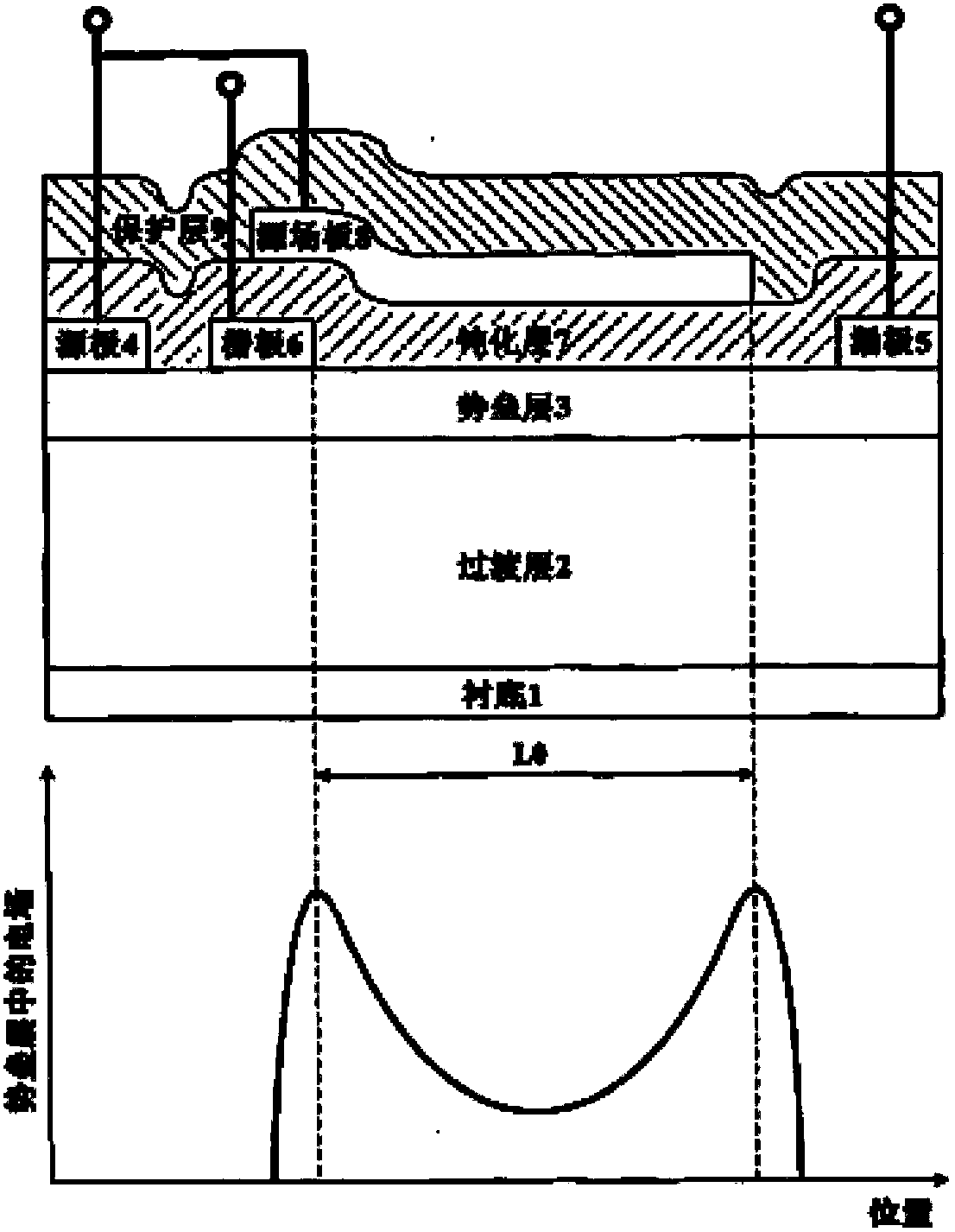
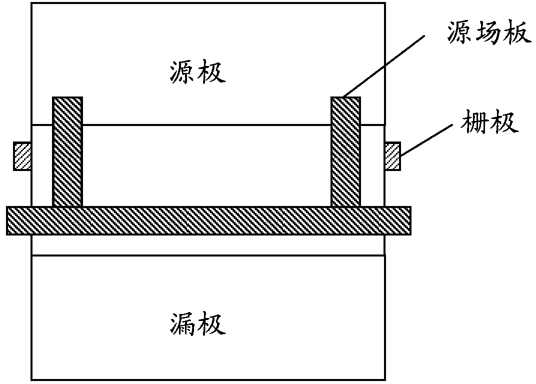
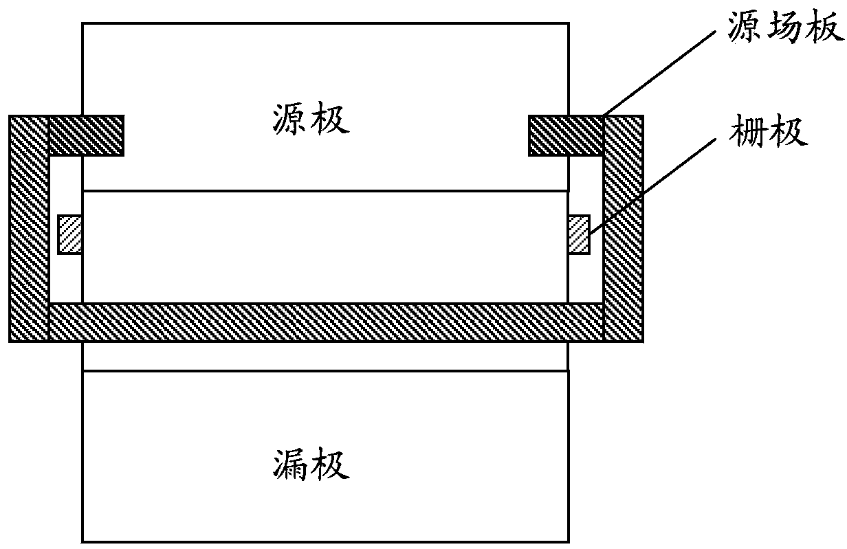
[0060] As stated in the background art, using a source field plate can increase the breakdown voltage of a semiconductor device, but at the same time it will increase the gate-source capacitance Cgs of the device, thereby deteriorating the frequency characteristic of the device. In order to reduce Cgs, ...


PUM


Abstract

The invention discloses a semiconductor device and a manufacturing method thereof. The device comprises a substrate, a multi-layer semiconductor layer positioned on the substrate, a source electrode and a drain electrode positioned on the multi-layer semiconductor layer, a grid electrode positioned between the source electrode and the drain electrode, as well as a dielectric layer positioned on at least one part of the surface of the multi-layer semiconductor layer arranged between the grid electrode and the drain electrode and a source field plate positioned on the dielectric layer, wherein a groove is formed in the dielectric layer, the source field plate is electrically connected to the source electrode through at least one conductive path, and the source field plate completely or partially covers the groove in the dielectric layer. The semiconductor device and the manufacturing method thereof provided by the invention have the advantages that the source field plate is given a full play, grid source capacitance Cgs is reduced, a peak value electric field at the edge of the grid electrode is reduced, the breakdown voltage of the device is improved, the grid leakage current of the device is reduced, the frequency characteristic of the device is improved, and the advantage of the high output power of the device is fully played.

Description

technical field [0001] The invention relates to the technical field of microelectronics, in particular to a semiconductor device with a source field plate and a manufacturing method thereof. Background technique [0002] III-V compound semiconductor materials, such as gallium nitride-based semiconductor materials, gallium arsenide-based semiconductor materials and indium phosphide-based semiconductor materials, etc., their band gaps are often different, and people often use This feature forms various heterojunction structures. This heterojunction structure has a characteristic that a quantum potential well and a high-concentration two-dimensional electron gas can be generated near the heterojunction interface. This two-dimensional electron gas is bound in the quantum In the potential well, the separation of carriers and ionized impurities in space is realized, the Coulomb force of ionized impurities on carriers is reduced, and the influence of ionized scattering centers is e...

Claims


Application Information

Patent Timeline
IPC IPC(8): H01L29/40H01L21/28H01L29/778H01L21/335
Inventor 张乃千裴风丽
Owner DYNAX SEMICON
Why Eureka
Try Eureka