Thin film transistor and method of fabricating the same

a thin film transistor and gate insulating layer technology, applied in semiconductor devices, photovoltaic energy generation, solid-state devices, etc., can solve the problems of poor contact resistance between the source/drain electrode and the gate insulating layer, and achieve good adhesion, good adhesion, and improved contact resistance

Active Publication Date: 2006-02-09
SAMSUNG DISPLAY CO LTD
View PDF5 Cites 33 Cited by
  • Summary
  • Abstract
  • Description
  • Claims
  • Application Information

AI Technical Summary

Benefits of technology

[0009] It is therefore an object of the present invention to provide an improved design for a bottom-contact OTFT.

Problems solved by technology

Even though bottom contact OTFTs are preferred over top-contact OTFTs, bottom-contact OTFTs still have many deficiencies.
For example, the adhesion between the source / drain electrodes and the underlying gate insulating layer is weak, the contact resistance between the source / drain electrodes and the gate insulating layer is poor and a gate leakage current occurs through the organic gate insulating layer because of pinhole failure.

Method used


Image

  • Thin film transistor and method of fabricating the same
  • Thin film transistor and method of fabricating the same
  • Thin film transistor and method of fabricating the same

Examples


first embodiment

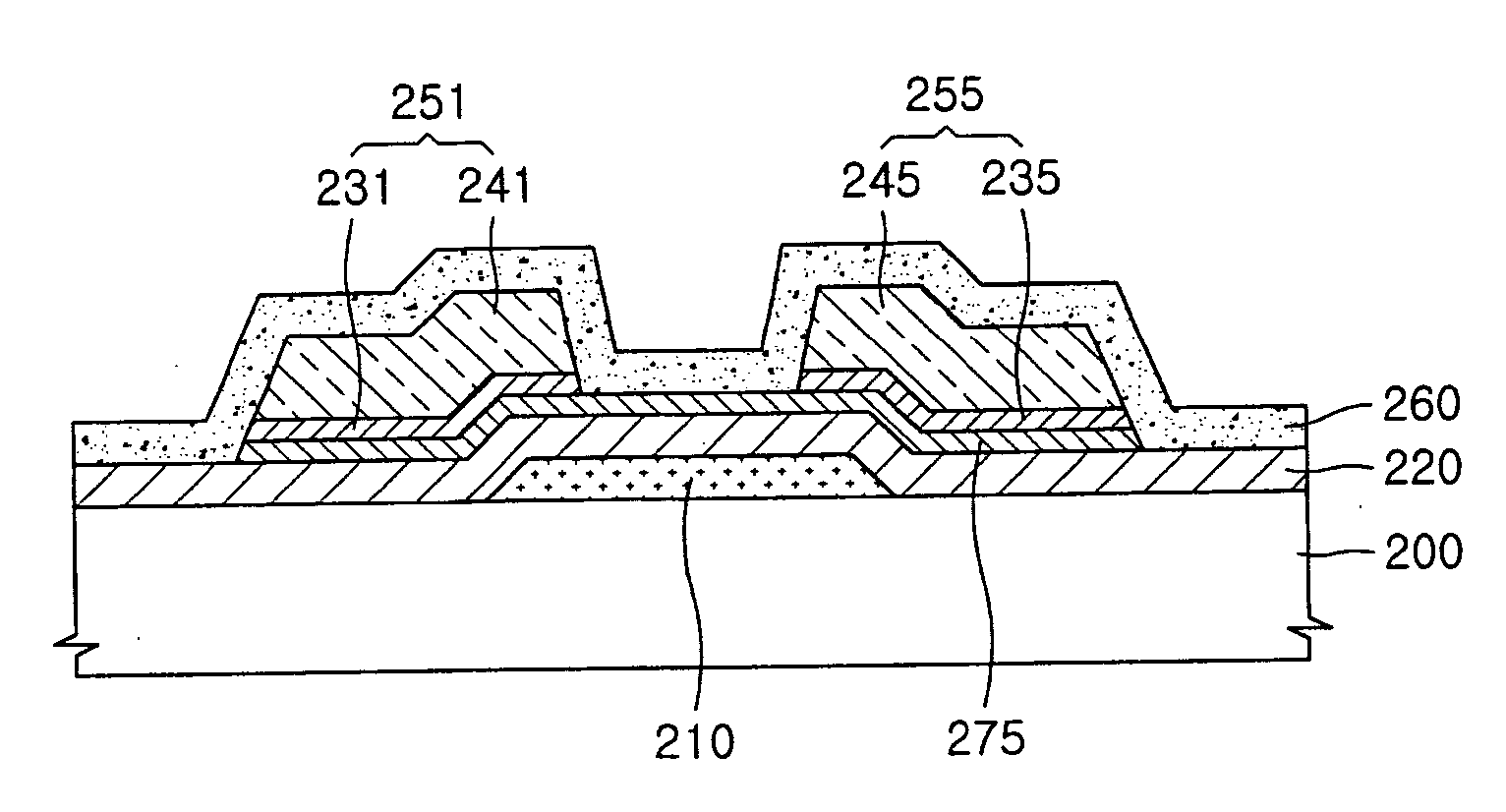
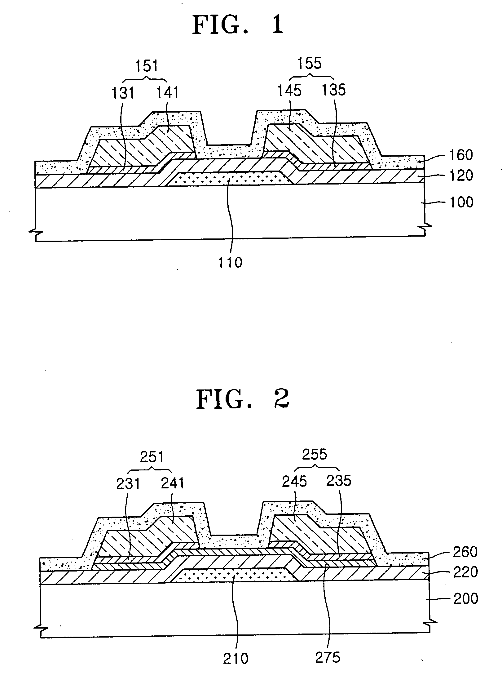
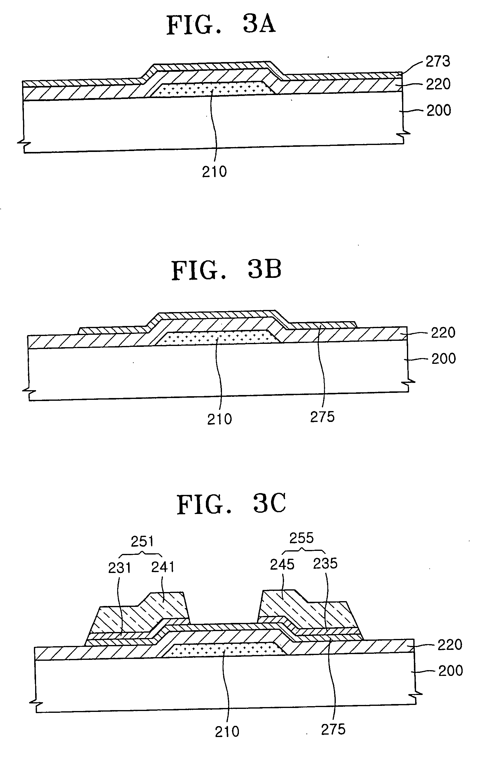
[0034] Turning now to FIG. 2, FIG. 2 is a cross-sectional view of an organic thin film transistor (OTFT) according to the present invention. Referring to FIG. 2, a gate electrode 210 is formed on portions of the substrate 200 and a gate insulating layer 220 is formed on the gate electrode 210 and on remaining exposed portions of the substrate 200. An adhesive layer 275 is formed on the gate insulating layer 220 and source / drain electrodes 251 and 255 are formed on portions of the adhesive layer 275 leaving other portions of the adhesive layer 275 that corresponds to the gate electrode 210 exposed. A semiconductor layer 260 having a predetermined conduction type, for example p-type, is formed on the source / drain electrodes 251 and 255 and on the exposed portions of the adhesive layer 275.

[0035] The substrate 200 can be made of glass or silicon. The substrate 200 can instead be made of plastics, such as polyethylene terephthalate (PET), polyethylene naphthalate (PEN), polyether sulfon...

second embodiment

[0051] Turning now to FIG. 5, FIG. 5 is a cross-sectional view of an organic thin film transistor (OTFT) according to the present invention. The OTFT illustrated in FIG. 5 has the same cross-sectional structure as in FIG. 2 except that the source / drain electrodes are made of the electrode layers only and do not include the binding layers 231 and 235.

[0052] Referring now to FIG. 5, a gate electrode 310 is formed on a substrate 300 and a gate insulating layer 320 is formed on the gate electrode 310 and on exposed portions of the substrate 300. An adhesive layer 375 is formed on the gate insulating layer 320 and source / drain electrodes 351 and 355 are formed on the adhesive layer 375. Between the source electrode 351 and the drain electrode 355 remains an exposed portion of the adhesive layer 375 that corresponds to the gate electrode 310. A semiconductor layer 360 is formed on top of the resultant structure, including the source / drain electrodes 351 and 355 and the exposed portion of ...


PUM

PropertyMeasurementUnit
adhesionaaaaaaaaaa
work functionaaaaaaaaaa
insulatingaaaaaaaaaa

Abstract

An organic thin film transistor (OTFT) having an adhesive layer and a method of fabricating the same. The OTFT includes a gate electrode formed on a substrate, a gate insulating layer formed on the gate electrode and on remaining exposed portions of the substrate, an adhesive layer formed on the gate insulating layer, source / drain electrodes formed on the adhesive layer, and a semiconductor layer formed on the source / drain electrodes and on the adhesive layer. The gate insulating layer and the semiconductor layer are organic, the adhesive layer providing adhesion between the source / drain electrodes and the gate insulating film while preventing gate leakage current while also improving contact resistance.

Description

CLAIM OF PRIORITY [0001] This application makes reference to, incorporates herein, and claims all benefits accruing under 35 U.S.C. §119 from an application for THIN FILM TRANSISTOR AND METHOD OF FABRICATING THE SAME earlier filed in the Korean Intellectual Property Office on Aug. 7, 2004 and there duly assigned Serial No. 2004-0062234. BACKGROUND OF THE INVENTION [0002] 1. Field of the Invention [0003] The present invention relates to a thin film transistor (TFT) and a method of fabricating the same, and more particularly, to an organic thin film transistor (OTFT) having improved adhesion between source / drain electrodes and a gate insulating layer with no gate leakage current caused by pinhole failure in the gate insulating layer. [0004] 2. Description of the Related Art [0005] OTFTs are driving elements expected to be used in next generation display devices. Active research is currently being conducted on OTFTs. OTFTs use a semiconductor layer made of an organic material and have ...

Claims


Application Information

Patent Timeline
Patent Type & Authority Applications(United States)
IPC IPC(8): H01L29/10H01L21/84
CPCH01L21/31691H01L51/0021H01L51/0034H01L51/0035H01L51/0036H01L51/0545H01L51/0052H01L51/0053H01L51/0097H01L51/0516H01L51/0037Y02E10/549H01L21/02118H10K71/60H10K85/10H10K85/111H10K85/1135H10K85/621H10K85/113H10K85/615H10K10/468H10K10/466H10K77/111
Inventor KOO, JAE-BONSUH, MIN-CHUL
Owner SAMSUNG DISPLAY CO LTD
Why Eureka
Try Eureka