Programmable array logic or memory devices with asymmetrical tunnel barriers

a technology of asymmetric tunnel barriers and programmable arrays, applied in semiconductor devices, transistors, instruments, etc., can solve problems such as premature breakdown and reliability problems, poor quality interpoly oxides, and localized high electric fields

Inactive Publication Date: 2005-02-03
MICRON TECH INC
View PDF69 Cites 153 Cited by
  • Summary
  • Abstract
  • Description
  • Claims
  • Application Information

AI Technical Summary

Benefits of technology

The above mentioned problems with programmable array type logic and/or memory devices and other problems are addressed by the present invention and will be understood by reading and st

Problems solved by technology

However, the rough top surface of the polysilicon floating gate resulted in, poor quality interpoly oxides, sharp points, localized high electric fields, premature breakdown and reliability problems.
However, in order to enable a reasonable write speed the ETOX cell uses channel hot electron injection, the erase operation which can be slower is achieved by Fowler-Nordhiem tunneling from the floating gate to the source.
The large barriers to electron tunneling or hot electron injection presented by the silicon oxide-silicon interface, 3.2 eV, result in slow write and erase speeds even at very high electric fields.
The combination of very high electric fields and damage by hot electron collisions in the oxide result in a number of operational

Method used


Image

  • Programmable array logic or memory devices with asymmetrical tunnel barriers
  • Programmable array logic or memory devices with asymmetrical tunnel barriers
  • Programmable array logic or memory devices with asymmetrical tunnel barriers

Examples


example i

Formation of Al2O3 Tunnel Barriers

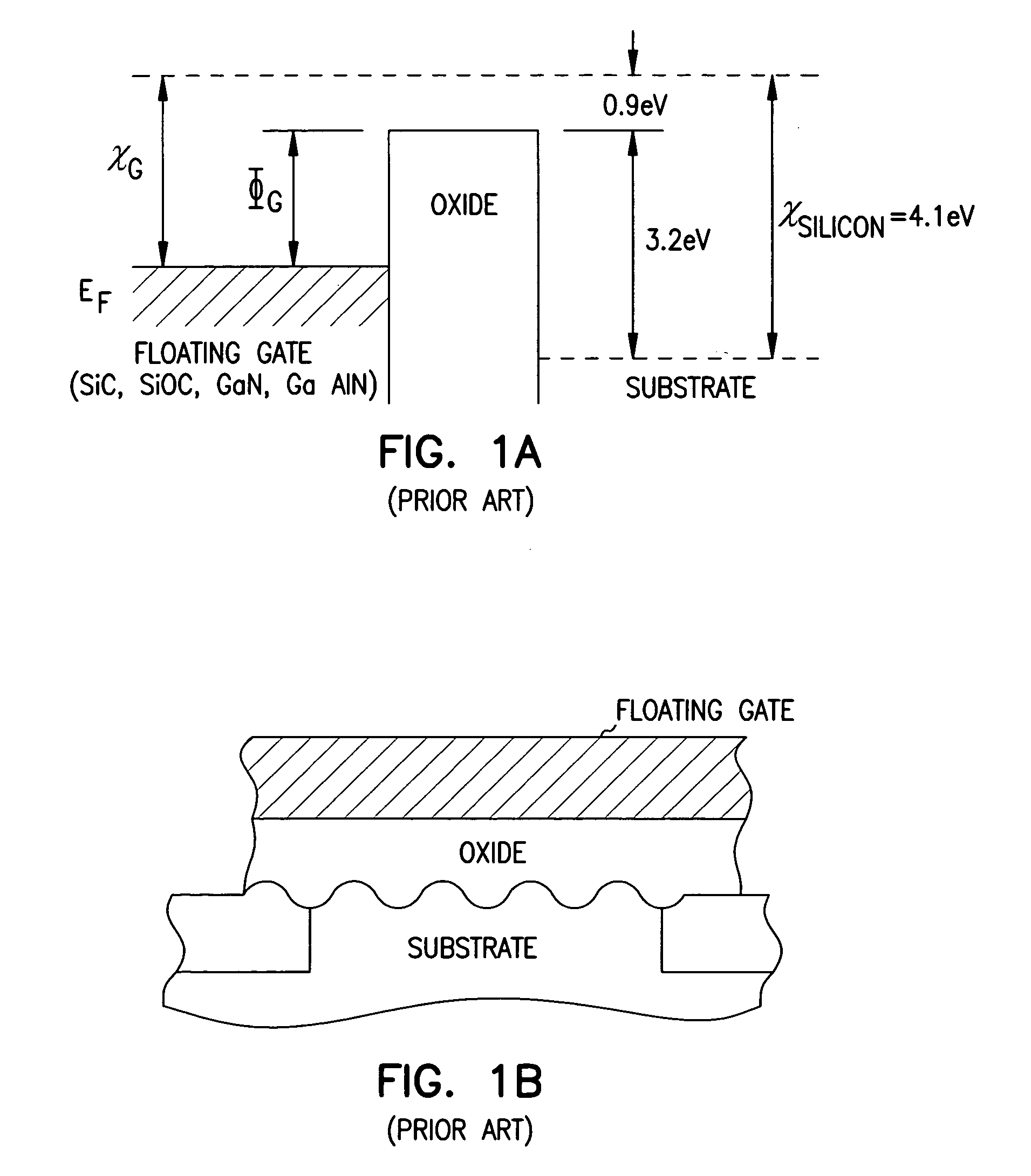
As stated above, the conventional large barrier insulating dielectrics are silicon oxide and silicon nitride. (See generally, T. P. Ma et al., “Tunneling leakage current in ultra-thin (<4 nm) nitride / oxide stack dielectrics,” IEEE Electron Device Letters, vol. 19, no. 10, pp. 388-390, 1998). The realities are that silicon oxide is not an optimum choice for memory type devices, because the 3.2 eV tunnel barrier is too high resulting in premature failure of the insulators and limiting the number of operational cycles to be in the order of 105 to 107.

According to one embodiment of the present invention, an asymmetrical low tunneling barrier interpoly insulator is used instead, such as Al2O3 with a tunneling barrier of approximately 2.0 eV. A number of studies have dealt with electron tunneling in Al / Al2O3 / Al structures where the oxide was grown by “low temperature oxidation” in either molecular or plasma oxygen. (See generally, S. M. Sze, Phys...

example ii

Formation of Single- and Multi-Layer Transition Metal Oxide Tunnel Barriers

The band gap energies and barrier heights of some conventional gate insulators as silicon oxide, silicon nitride and aluminum oxide as well as tantalum oxide have been investigated and described in detail (see generally, H. Itokawa et al., “Determination of bandgap and energy band alignment for high-dielectric-constant gate insulators using high-resolution x-ray photoelectron spectroscopy,” Ext. Abstracts Int. Conf. On Solid State Devices and Materials, pp. 158-159, 1999). Formation of single and double-layer dielectric layers of oxides of Ta2O5 and similar transition metal oxides can be accomplished by thermal as well as plasma oxidation of films of these metals. (See generally, H.F. Luan, et al., “High quality Ta2O5 gate dielectrics with Tox eq<10 Å,” International Electron Devices Meeting Technical digest, p. 141-144, 1999; J. Robertson and C. W. Chen, “Schottky barrier heights of tantalum oxide, ba...

example iii

Formation of Alternate Metal Compound Tunnel Barriers

Although no applications may be immediately obvious, it is conceivable that one might want to form a stack of asymmetrical oxide films having quite different properties, for example, a stack comprised of a high dielectric constant (k) oxide / a low k oxide / a high k oxide. “Low temperature oxidation” can be used to form numerous variations of such structures. While most of this disclosure deals with the formation and use of stacks of asymmetrical oxide dielectrics, it is also possible to use “low temperature oxidation” to form other thin film dielectrics such as nitrides, oxynitrides, etc. that could provide additional functions such as being altered by monochromatic light, etc. These will not be discussed further here.


PUM


Abstract

Structures and methods for programmable array type logic and/or memory devices with asymmetrical low tunnel barrier intergate insulators are provided. The programmable array type logic and/or memory devices include non-volatile memory which has a first source/drain region and a second source/drain region separated by a channel region in a substrate. A floating gate opposing the channel region and is separated therefrom by a gate oxide. A control gate opposes the floating gate. The control gate is separated from the floating gate by an asymmetrical low tunnel barrier intergate insulator. The asymmetrical low tunnel barrier intergate insulator includes a metal oxide insulator selected from the group consisting of Al2O3, Ta2O5, TiO2, ZrO2, Nb2O5, SrBi2Ta2O3, SrTiO3, PbTiO3, and PbZrO3. The floating gate includes a polysilicon floating gate having a metal layer formed thereon in contact with the low tunnel barrier intergate insulator. And, the control gate includes a polysilicon control gate having a metal layer, having a different work function from the metal layer formed on the floating gate, formed thereon in contact with the low tunnel barrier intergate insulator.

Description

FIELD OF THE INVENTION The present invention relates generally to integrated circuits, and in particular to programmable array type logic and / or memory devices with asymmetrical low tunnel barrier interpoly insulators. BACKGROUND OF THE INVENTION Flash memories have become widely accepted in a variety of applications ranging from personal computers, to digital cameras and wireless phones. Both INTEL and AMD have separately each produced about one billion integrated circuit chips in this technology. The original EEPROM or EARPROM and flash memory devices described by Toshiba in 1984 used the interpoly dielectric insulator for erase. (See generally, F. Masuoka et al., “A new flash EEPROM cell using triple polysilicon technology,” IEEE Int. Electron Devices Meeting, San Francisco, pp. 464-67, 1984; F. Masuoka et al., “256K flash EEPROM using triple polysilicon technology,” IEEE Solid-State Circuits Conf., Philadelphia, pp. 168-169, 1985). Various combinations of silicon oxide and si...

Claims


Application Information

Patent Timeline
IPC IPC(8): G11C16/04H01L21/8247H01L27/115H01L29/51H01L29/788
CPCG11C16/0416H01L27/115H01L29/7885H01L29/51H01L29/511H01L27/11556H10B41/27H10B69/00
Inventor FORBES, LEONARDELDRIDGE, JEROME M.AHN, KIE Y.
Owner MICRON TECH INC
Why Eureka
Try Eureka