Metal gate MOS transistors and methods for making the same

a technology of metal gate mos and transistor, which is applied in the direction of semiconductor devices, basic electric elements, electrical equipment, etc., can solve the problems of not being able to adjust the work function value of tin gate, not being able to achieve the optimization of pmos or nmos transistor work functions, and not being able to achieve large-scale adjustment of work functions, so as to reduce process time, reduce cost, and reduce process tim

Inactive Publication Date: 2005-08-30
TEXAS INSTR INC
View PDF23 Cites 175 Cited by
  • Summary
  • Abstract
  • Description
  • Claims
  • Application Information

AI Technical Summary

Benefits of technology

[0016]One aspect of the invention advantageously allows the use of a single starting material for the metal gate contact portion of the gate structures of both PMOS and NMOS devices, where the starting material is a metal boride or a metal nitride. The metal boride may be any boron-containing metal material, including alloys, and the metal nitride may be any nitrogen-containing metal or nitrogen-containing metal alloy. The starting material is provided with boron or nitrogen in one of the PMOS and NMOS regions through implantation, diffusion, or other suitable techniques, either before or after poly-silicon or tungsten formation, and before or after gate patterning. The change in the boron or nitrogen content of the starting material provides adjustment of the material work function, thereby tuning the threshold voltage of at least one of the resulting PMOS or NMOS transistors without significant channel engineering, and without the process complications inherent in using two different starting metal materials.
[0018]In another possible implementation, a starting material may be selected having an initial work function value near one of the desired gate work functions, and may then be provided with dopants to achieve the desired value without the need for substantial channel engineering. In this situation, channel engineering will only be needed for the other transistor type (e.g., PMOS or NMOS). For example, a mid-gap metal such as TiN with a work function of about 4.4 to 4.6 eV may be formed over the gate dielectrics in both NMOS and PMOS regions. The TiN in the PMOS region is then provided with boron to create a metal boride TiB2 having a work function of 4.9 eV, which is the desired PMOS value. As a result, little or no PMOS channel engineering is needed, thereby reducing process time, complexity, cost, etc., and also providing a further advantage in that less dopants are provided in the PMOS channel, which increases channel carrier mobility. Normal channel engineering can then be used to compensate the NMOS channel regions for the TiN gate work function in the NMOS transistors.
[0019]In yet another implementation, a metal boride is used as the starting material, and nitrogen is selectively introduced in the NMOS regions to provide a metal nitride having a different work function. For example, TiB2 may be initially formed, having the desired 4.9 eV work function for PMOS devices. The TiB2 in the NMOS regions is then nitrided to create TiN, wherein channel engineering can again be used to adjust the NMOS channel work function accordingly. The invention thus provides for the possibility of using a single starting material, and the possibility of eliminating or simplifying the channel engineering for at least one of the transistor types, while also realizing the other advantages of metal gates (e.g., higher conductivity, minimum depletion, etc.).

Problems solved by technology

Furthermore, most metals suitable for use in transistor gate designs do not inherently have one of the two desired work functions.
Thus, the work function of a TiN gate is not optimized for either PMOS or NMOS transistors.
PMOS and NMOS channel engineering can be used to compensate for such a gate design, but these techniques are primarily used for fine tuning the gate to substrate work function difference, and are not generally suitable for large adjustments in work function values.
Furthermore, it is desirable to avoid gate processing which uses two separate metals, as etch processing and other fabrication steps may be hard to optimize for two different metals.

Method used


Image

  • Metal gate MOS transistors and methods for making the same
  • Metal gate MOS transistors and methods for making the same
  • Metal gate MOS transistors and methods for making the same

Examples


Embodiment Construction

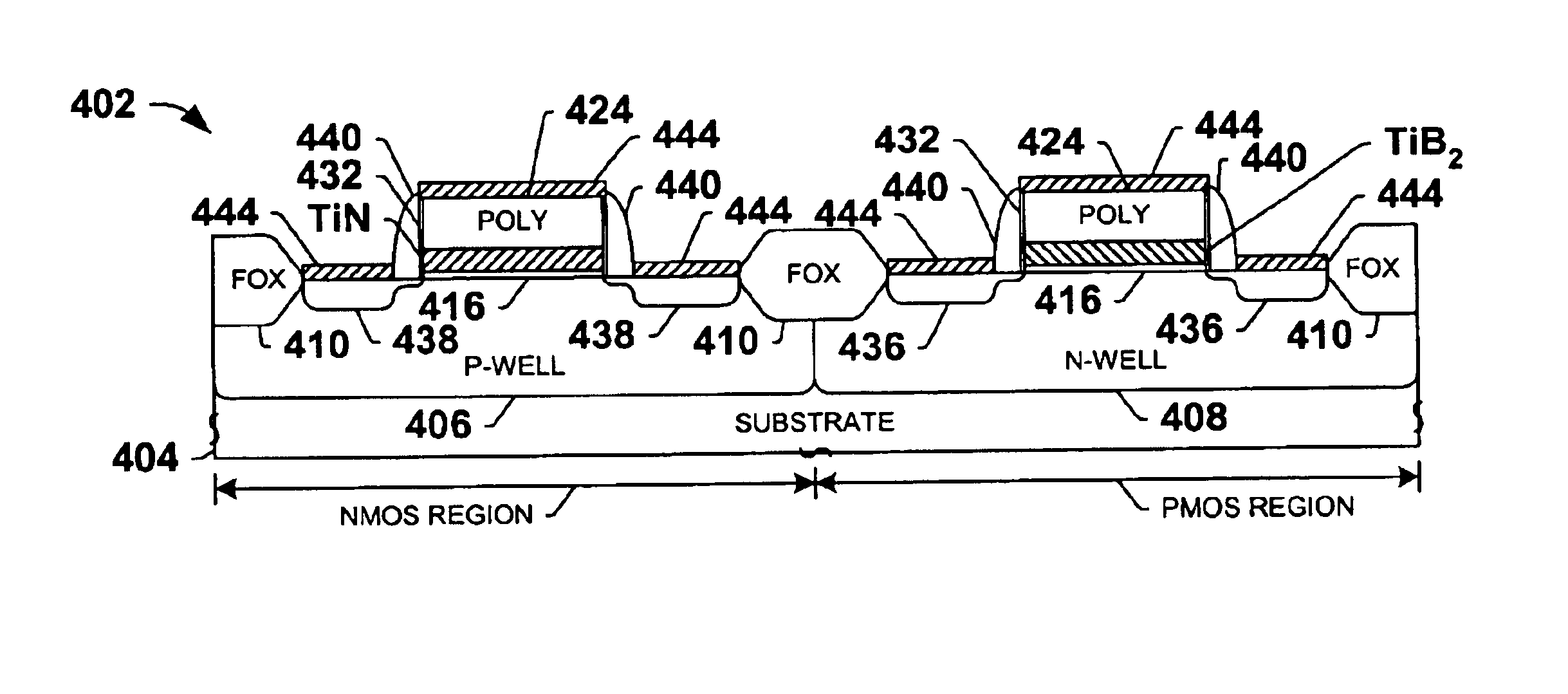
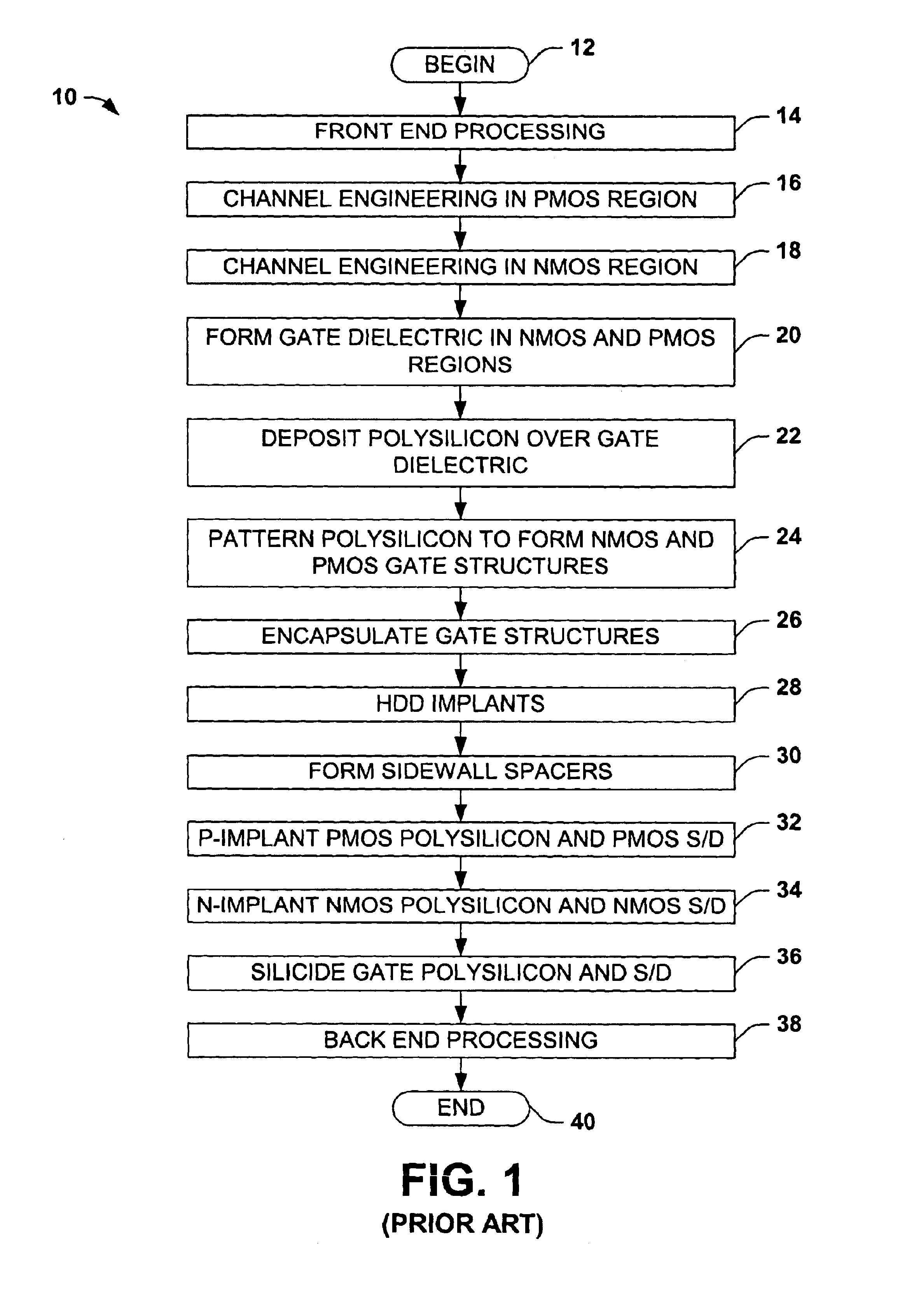
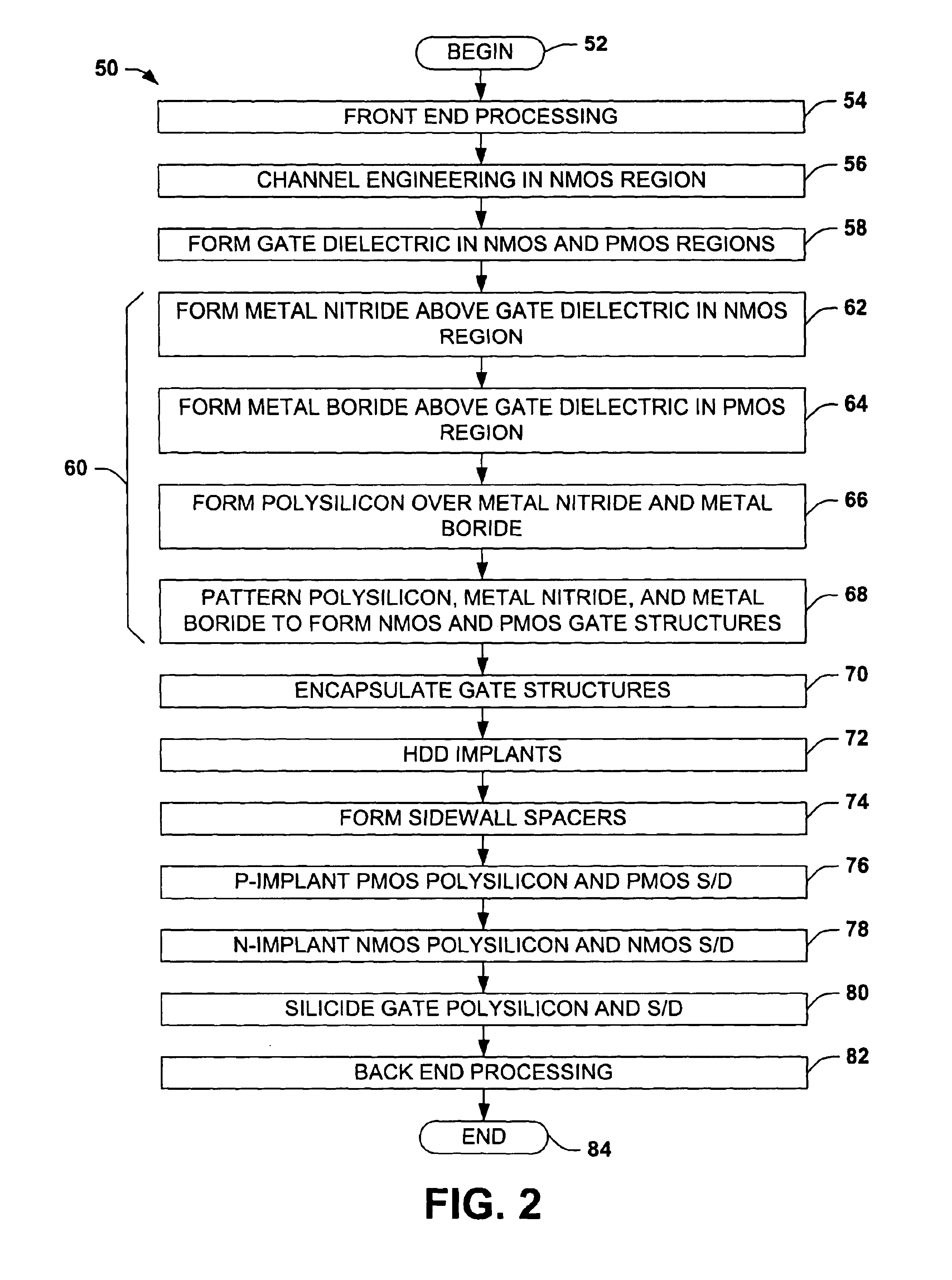
[0026]One or more implementations of the present invention will now be described with reference to the attached drawings, wherein like reference numerals are used to refer to like elements throughout, and wherein the illustrated structures are not necessarily drawn to scale. The invention relates to metal gate CMOS devices and fabrication methods in which metal nitride and metal boride gate contact materials are used for NMOS and PMOS transistors, respectively. The invention may be employed to simplify channel engineering steps in particular, and fabrication processing generally, while mitigating or eliminating the poly depletion shortcomings of conventional CMOS devices, and without having to use different metal starting materials in gate fabrication.

[0027]In the methods and devices of the invention, metal nitride is formed above a gate dielectric in an NMOS region and metal boride is formed above the gate dielectric in a PMOS region, wherein these and the gate dielectric may be fo...


PUM

PropertyMeasurementUnit
work functionaaaaaaaaaa

Abstract

Semiconductor devices and fabrication methods are provided, in which metal transistor gates are provided for MOS transistors. Metal boride is formed above a gate dielectric to create PMOS gate structures and metal nitride is formed over a gate dielectric to provide NMOS gate structures. The metal portions of the gate structures are formed from an initial starting material that is either a metal boride or a metal nitride, after which the starting material is provided with boron or nitrogen in one of the PMOS and NMOS regions through implantation, diffusion, or other techniques, either before or after formation of the conductive upper material, and before or after gate patterning. The change in the boron or nitrogen content of the starting material provides adjustment of the material work function, thereby tuning the threshold voltage of the resulting PMOS or NMOS transistors.

Description

FIELD OF INVENTION[0001]The present invention relates generally to semiconductor devices and more particularly to metal gate MOS transistor devices and fabrication methods for making the same.BACKGROUND OF THE INVENTION[0002]Field effect transistors (FETs) are widely used in the electronics industry for switching, amplification, filtering, and other tasks related to both analog and digital electrical signals. Most common among these are metal-oxide-semiconductor field-effect transistors (MOSFETs), wherein a gate contact or electrode is energized to create an electric field in a channel region of a semiconductor body, by which electrons are allowed to travel through the channel between a source region and a drain region of the semiconductor body. The source and drain regions are typically formed by adding dopants to targeted regions on either side of the channel. A gate dielectric or gate oxide is formed over the channel, and a gate electrode or gate contact is formed over the gate d...

Claims


Application Information

Patent Timeline
Patent Type & Authority Patents(United States)
IPC IPC(8): H01L21/28H01L21/70H01L21/02H01L29/49H01L21/8238H01L29/40H01L21/336H01L29/51
CPCH01L21/28088H01L21/823842H01L29/4966H01L29/513H01L29/517H01L29/665
Inventor VISOKAY, MARKCOLOMBO, LUIGICHAMBERS, JAMES J.
Owner TEXAS INSTR INC
Why Eureka
Try Eureka