Semiconductor cleaning device and semiconductor cleaning method

a cleaning device and semiconductor technology, applied in the direction of suction cleaners, cleaning equipments, chemistry apparatus and processes, etc., can solve the problems of deteriorating the yield of the semiconductor device, difficult to remove the foreign matter adhered to the side surface of the semiconductor wafer, so as to prevent the re-adhesion of the removed foreign matter

Active Publication Date: 2013-06-20
MITSUBISHI ELECTRIC CORP
View PDF0 Cites 5 Cited by
  • Summary
  • Abstract
  • Description
  • Claims
  • Application Information

AI Technical Summary

Benefits of technology

[0010]The present invention has been made in view of the above problems, and an abject thereof is to provide a semiconductor cleaning device and a semiconductor cleaning method that can remove foreign matter adhered to a side surface of a semiconductor device, and can prevent re-adhesion of the removed foreign matter.
[0012]According to the semiconductor cleaning device of the invention, since the external electrode is opposed to the side surface of the semiconductor device, the external electrode can remove the foreign matter adhered to the side surface of the semiconductor device from the side surface. Since the suction means can take in the foreign matter through the opening arranged below the side surface of the semiconductor device, it is possible to prevent re-adhesion of the foreign matter that was removed from the side surface of the semiconductor device.

Problems solved by technology

In the processing of manufacturing the semiconductor devices, entry of foreign matter occurs in various steps to cause disadvantages in the semiconductor devices.
This deteriorates a yield of the semiconductor devices.
However, in the device disclosed in the above Japanese Patent Laying-Open No. 11-087457, since the foreign matter is transferred onto the plate member from the portion of the electrostatically attracting and transporting arm that is in contact with the rear surface of the wafer, it is impossible to remove the foreign matter adhered to a side surface of the semiconductor wafer.
In the device disclosed in the above Japanese Patent Laying-Open No. 2011-099156, since the electrostatic chuck attracts the rear surface of the semiconductor wafer, it is difficult to remove the foreign matter adhered to a side surface of the semiconductor wafer.
Each of the semiconductor devices which produced by dividing the semiconductor wafer by dicing or the like may suffer from a problem due to presence of the foreign matter in test steps such as evaluation of electric characteristics after the manufacturing steps.
For example, when foreign matter adheres to the surface of the semiconductor device provided with a pad for electric connection, it may cause short-circuiting and discharging.
These cause disadvantages in the semiconductor device.
The deterioration in close-contact property between the semiconductor device and the external electrode affects a contact resistance and consequently affects electric properties.
In a contact portion where the semiconductor device is in contact with the foreign matter as well as the vicinity thereof, the presence of the foreign matter may cause a defect such as a crack, and thereby may partially break the semiconductor device.

Method used


Image

  • Semiconductor cleaning device and semiconductor cleaning method
  • Semiconductor cleaning device and semiconductor cleaning method
  • Semiconductor cleaning device and semiconductor cleaning method

Examples


first embodiment

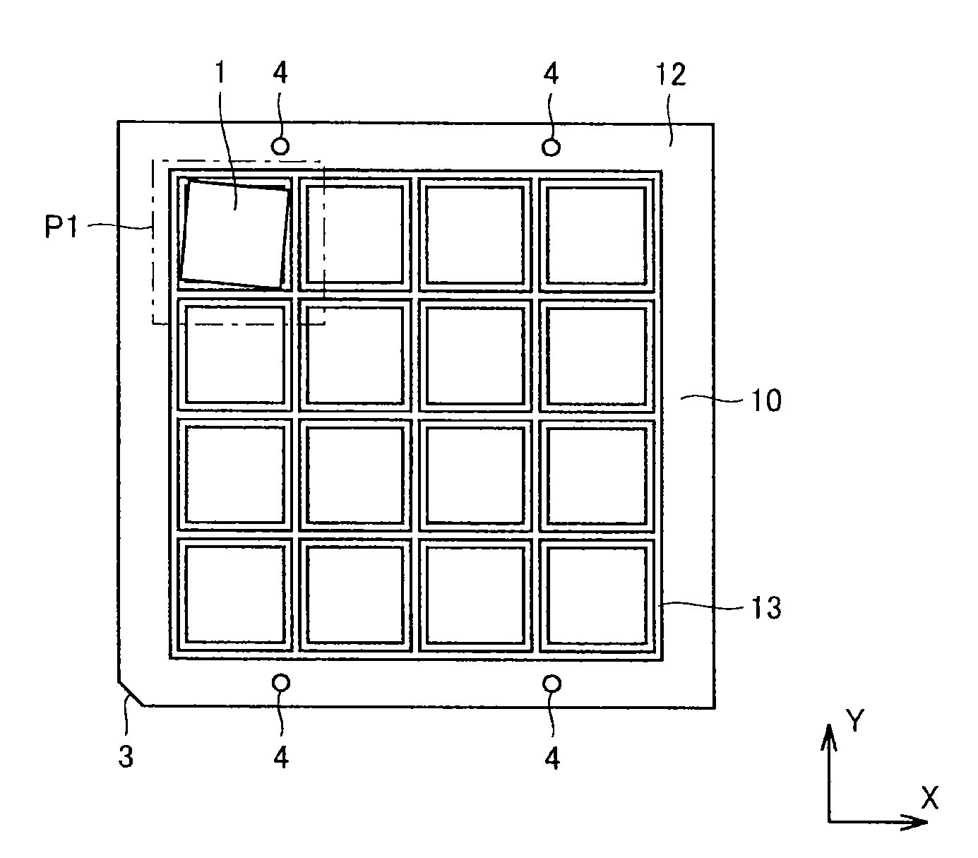
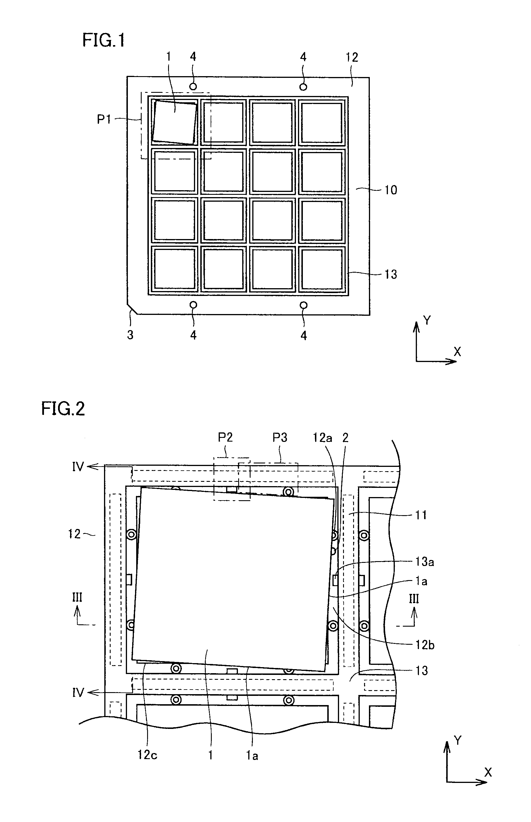
[0027]First, a structure of a semiconductor cleaning device of a first embodiment of the invention will be described.

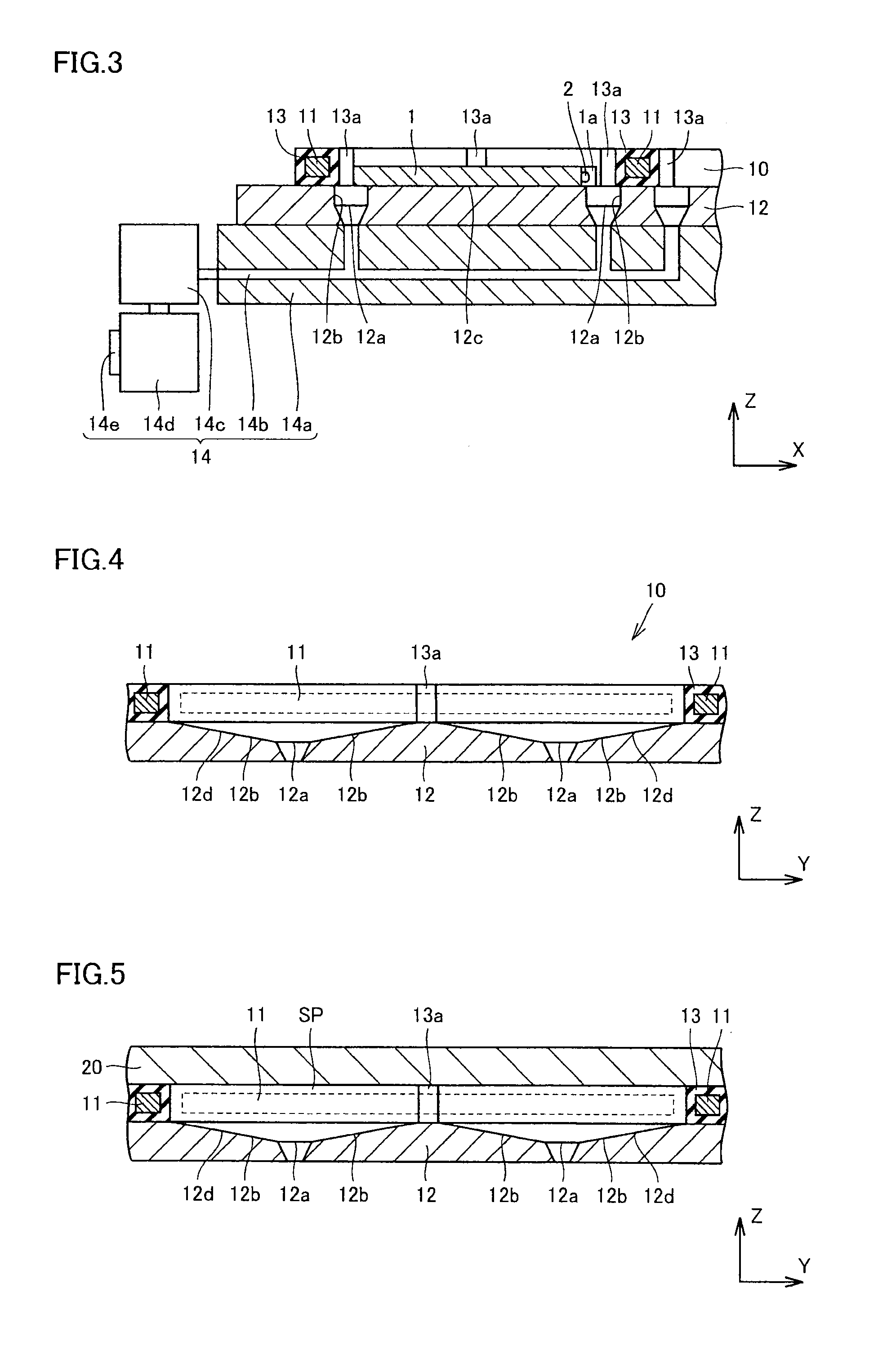
[0028]Referring to FIGS. 1 to 4, the semiconductor cleaning device of the embodiment is a device for removing foreign matter 2 from semiconductor devices 1. In FIGS. 1 to 3, semiconductor devices 1 are arranged on the semiconductor cleaning device. For the sake of clarification, FIG. 1 shows only one semiconductor device 1. FIGS. 1 and 2 do not show suction means for the sake of illustration. FIG. 2 shows a portion where one semiconductor device 1 is arranged. FIG. 4 does not show the suction means for the sake of clarification.

[0029]Semiconductor device 1 is, e.g., a semiconductor chip formed of a silicon substrate that is prepared by dicing a silicon wafer. Foreign matter 2 is small silicon pieces and silicon scraps that are present on a side surface 1a of semiconductor device 1.

[0030]The semiconductor cleaning device primarily includes an external electrode 11, a b...

second embodiment

[0077]A second embodiment of the invention is different from the first embodiment in that it includes charge erasing means.

[0078]Referring to FIG. 11, a semiconductor cleaning device of the embodiment includes charge erasing means for erasing electrostatic charges on foreign matter 2 adhered to semiconductor device 1. The charge erasing means may have an ionizer 23. Ionizer 23 is arranged on a top surface of cap 20. Ionizer 23 is configured such that it can erase the charges on foreign matter 2 by supplying positive and negative ions to the vicinity of frame 13 through through holes 21 formed in cap 20. Since charge-erased foreign matter 2 can be easily separated from frame 13, separated foreign matter 2 can be easily taken into opening 12a by starting in advance the air suction. Ionizer 23 may be of a DC-type or AC-type. The AC-type ionizer can alternately produce positive and negative ions, and the DC-type ionizer can produce ions of a predetermined sign from a dedicated electrode...


PUM

PropertyMeasurementUnit
electrically insulating propertyaaaaaaaaaa
voltagesaaaaaaaaaa
areaaaaaaaaaaa

Abstract

A semiconductor cleaning device includes an external electrode opposed to a side surface of the semiconductor device; a base configured to allow arrangement of the semiconductor device, and having an opening positioned between the side surface of the semiconductor device in the arranged state and the external electrode, and located below the side surface of the semiconductor device; a frame having an electrically insulating property, being in contact with the external electrode, arranged on the base and opposed to the side surface of the semiconductor device; and suction means connected to the opening in the base and being capable of taking in the foreign matter through the opening. Thereby, the semiconductor cleaning device and a semiconductor cleaning method that can remove the foreign matter adhered to the side surface of the semiconductor device and can prevent re-adhesion of the removed foreign matter can be obtained.

Description

BACKGROUND OF THE INVENTION[0001]1. Field of the Invention[0002]The present invention relates to a semiconductor cleaning device and a semiconductor cleaning method, and particularly to a semiconductor cleaning device and a semiconductor cleaning method for removing foreign matter from a semiconductor device.[0003]2. Description of the Background Art[0004]Semiconductor devices are manufactured through a multiple kinds of processing performed on a semiconductor wafer that is an aggregate of semiconductor devices. In the processing of manufacturing the semiconductor devices, entry of foreign matter occurs in various steps to cause disadvantages in the semiconductor devices. This deteriorates a yield of the semiconductor devices. Therefore, it is desired to remove the foreign matter from the semiconductor devices.[0005]For example, Japanese Patent Laying-Open Nos. 11-087457 and 2011-099156 have proposed devices that can remove foreign matter in a manufacturing process of semiconductor ...

Claims


Application Information

Patent Timeline
Patent Type & Authority Applications(United States)
IPC IPC(8): B08B6/00
CPCH01L21/67028H01L21/02076H01L21/67333B08B5/04B08B6/00H01L21/02041H01L21/02046H01L21/67H01L21/673
Inventor OKADA, AKIRANOGUCHI, TAKAYAAKIYAMA, HAJIME
Owner MITSUBISHI ELECTRIC CORP
Why Eureka
Try Eureka