Determining alignment using a spatially varying charge distribution

Active Publication Date: 2013-06-20
ORACLE INT CORP
View PDF1 Cites 2 Cited by
  • Summary
  • Abstract
  • Description
  • Claims
  • Application Information

AI Technical Summary

Benefits of technology

[0015]Another embodiment provides a system that includes the semiconductor die and the other semiconductor die. Moreover, the other semiconductor die may include a spatial alignment sensor proximate to a surface of the other semiconductor die. This spatial alignment sensor may detect an electrical field (or an associated electrical potential) associated with the spatially varying electric charge distribution, thereby facilitating determination of the spatial alignment in more than one direction between the semiconductor die and the other semiconductor die. Note that the spatial alignment transducer and the spatial alignment sensor may define the Vernier structure.
[0016]Another embodiment provides a metho

Problems solved by technology

If misalignment occurs, for example, at initial assembly or during system operation, channel crosstalk and potential bit errors can result.
However, these techniques usually involve measuring the physical misalignment using on-chip position sensors.
These currents are comparable to transistor leakage currents, which can compromise measurement accuracy.
Furthermore, this problem is expected to become progressively worse as critical dimensions are scaled to 90 nm and beyond, where the leakage currents can dominate the small signal currents, which may mak

Method used


Image

  • Determining alignment using a spatially varying charge distribution
  • Determining alignment using a spatially varying charge distribution
  • Determining alignment using a spatially varying charge distribution

Examples


Example

[0028]Note that like reference numerals refer to corresponding parts throughout the drawings. Moreover, multiple instances of the same part are designated by a common prefix separated from an instance number by a dash.

DETAILED DESCRIPTION

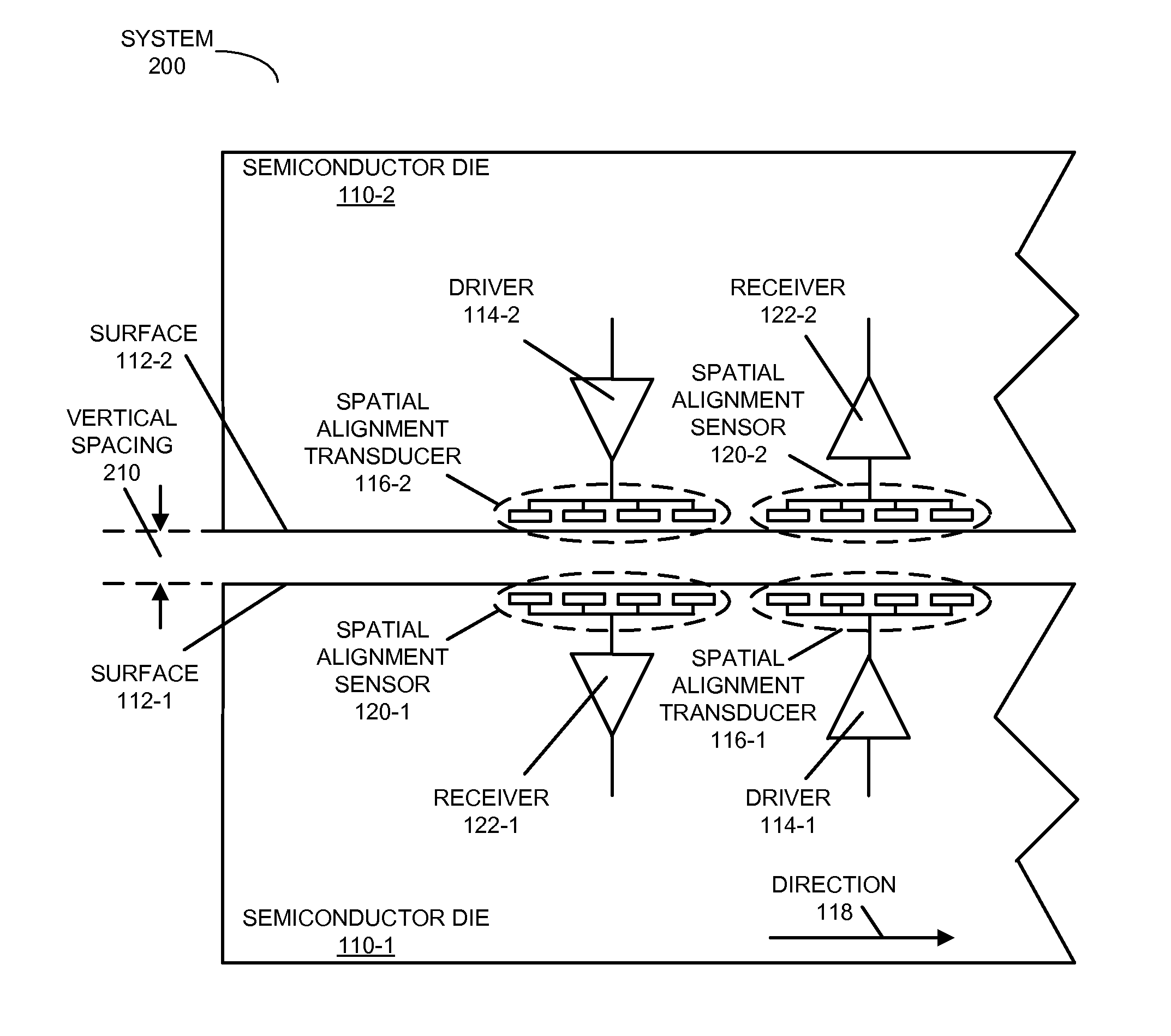
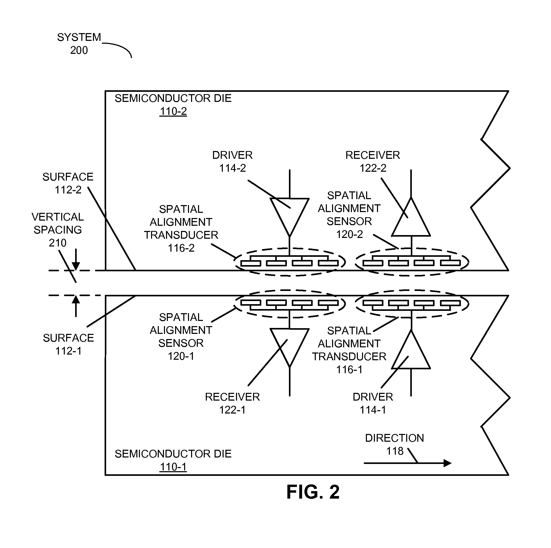
[0029]Embodiments of a semiconductor die, a system that includes the semiconductor die and another semiconductor die, and a method for determining the spatial alignment between the two semiconductor dies are described. This semiconductor die includes a driver, and a spatial alignment transducer that is electrically coupled to the driver and which is proximate to a surface of the semiconductor die. The driver establishes a spatially varying electric charge distribution in at least one direction in the spatial alignment transducer, thereby facilitating determination of a spatial alignment between the semiconductor die and the other semiconductor die. In particular, a spatial alignment sensor proximate to the surface of the other semiconductor die may ...


PUM


Abstract

A semiconductor die is described. This semiconductor die includes a driver, and a spatial alignment transducer that is electrically coupled to the driver and which is proximate to a surface of the semiconductor die. The driver establishes a spatially varying electric charge distribution in at least one direction in the spatial alignment transducer, thereby facilitating determination of a spatial alignment in more than one direction between the semiconductor die and another semiconductor die. In particular, a spatial alignment sensor proximate to the surface of the other semiconductor die may detect an electrical field (or an associated electrostatic potential) associated with the spatially varying electric charge distribution. This detected electric field may allow the vertical spacing between the surfaces of the semiconductor dies and/or an angular alignment of the semiconductor dies to be determined.

Description

CROSS REFERENCE TO RELATED APPLICATIONS[0001]This application is related to U.S. patent application Ser. No. 13 / 253,893, entitled “Determining Spacing Using a Spatially Varying Charge Distribution,” by Ivan E. Sutherland, having attorney docket number SUN10-0359-US-NP-1, filed 5 Oct., 2011, the contents of which is herein incorporated by reference.BACKGROUND[0002]1. Field[0003]The present disclosure generally relates to the design of a semiconductor die. More specifically, the present disclosure relates to a semiconductor die that includes a spatial alignment transducer with a spatially varying electric charge distribution that facilitates determining a spatial alignment between the semiconductor die and another semiconductor die.[0004]2. Related Art[0005]Proximity communication (PxC) is an input / output (I / O) technology that allows two face-to-face chips to communicate without wires. Although it promises much higher I / O density and lower power, chips that communicate using PxC typic...

Claims


Application Information

Patent Timeline
IPC IPC(8): G01N27/00H01L23/58
CPCH01L23/585H01L2224/83851H01L2225/06531H01L2225/06593H01L25/0657H01L2224/32145H01L2224/293H01L2224/16145H01L2224/131H01L2224/13021H01L24/72H01L24/32H01L2224/16147H01L2224/292H01L24/13H01L24/16H01L24/29H01L2924/014H01L2924/00014
Inventor CHOW, ALEXDROST, ROBERT J.HO, RONALDHOPKINS, ROBERT D.SUTHERLAND, IVAN E.
Owner ORACLE INT CORP
Why Eureka
Try Eureka