Non-volatile memory (NVM) and logic integration

a technology of logic and non-volatile memory, applied in the field of non-volatile memory (nvms), can solve the problem of unfavorable logic performance sacrifice in favor of nvm performan

Active Publication Date: 2013-07-04
NXP USA INC
View PDF7 Cites 35 Cited by
  • Summary
  • Abstract
  • Description
  • Claims
  • Application Information

AI Technical Summary

Problems solved by technology

In such cases it is undesirable to sacrifice logic performance in favor of performance of the NVM.

Method used


Image

  • Non-volatile memory (NVM) and logic integration
  • Non-volatile memory (NVM) and logic integration
  • Non-volatile memory (NVM) and logic integration

Examples


Embodiment Construction

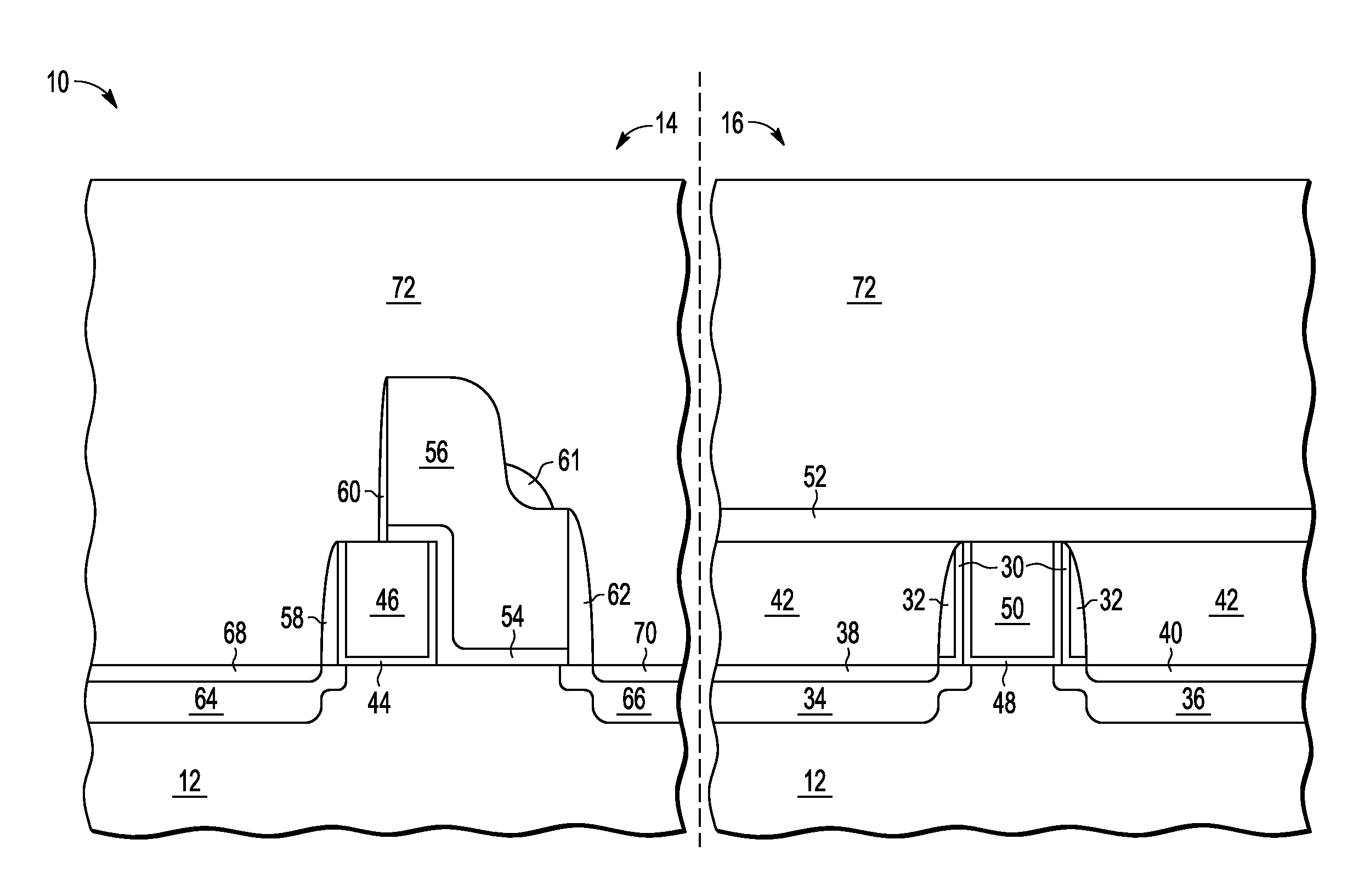
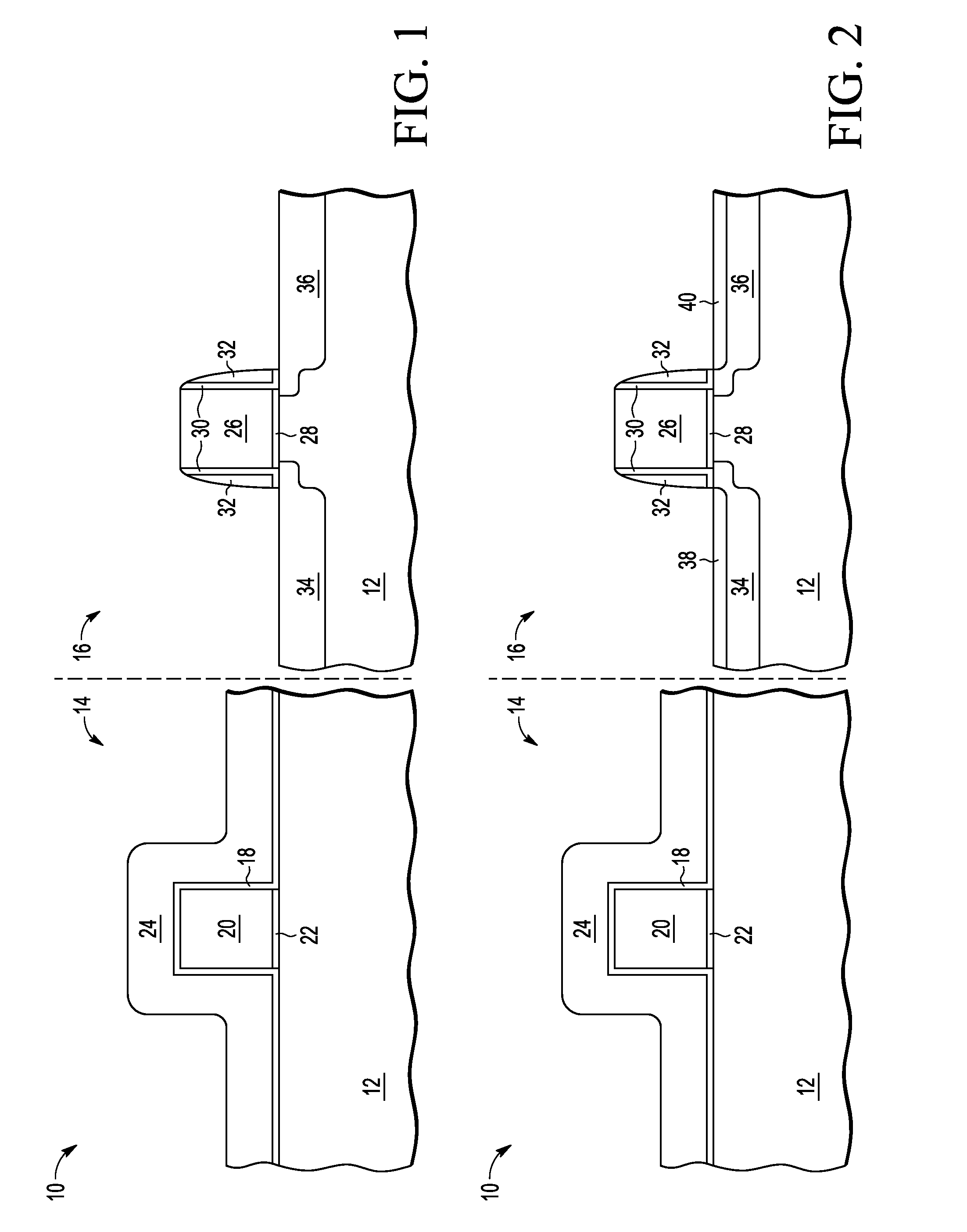
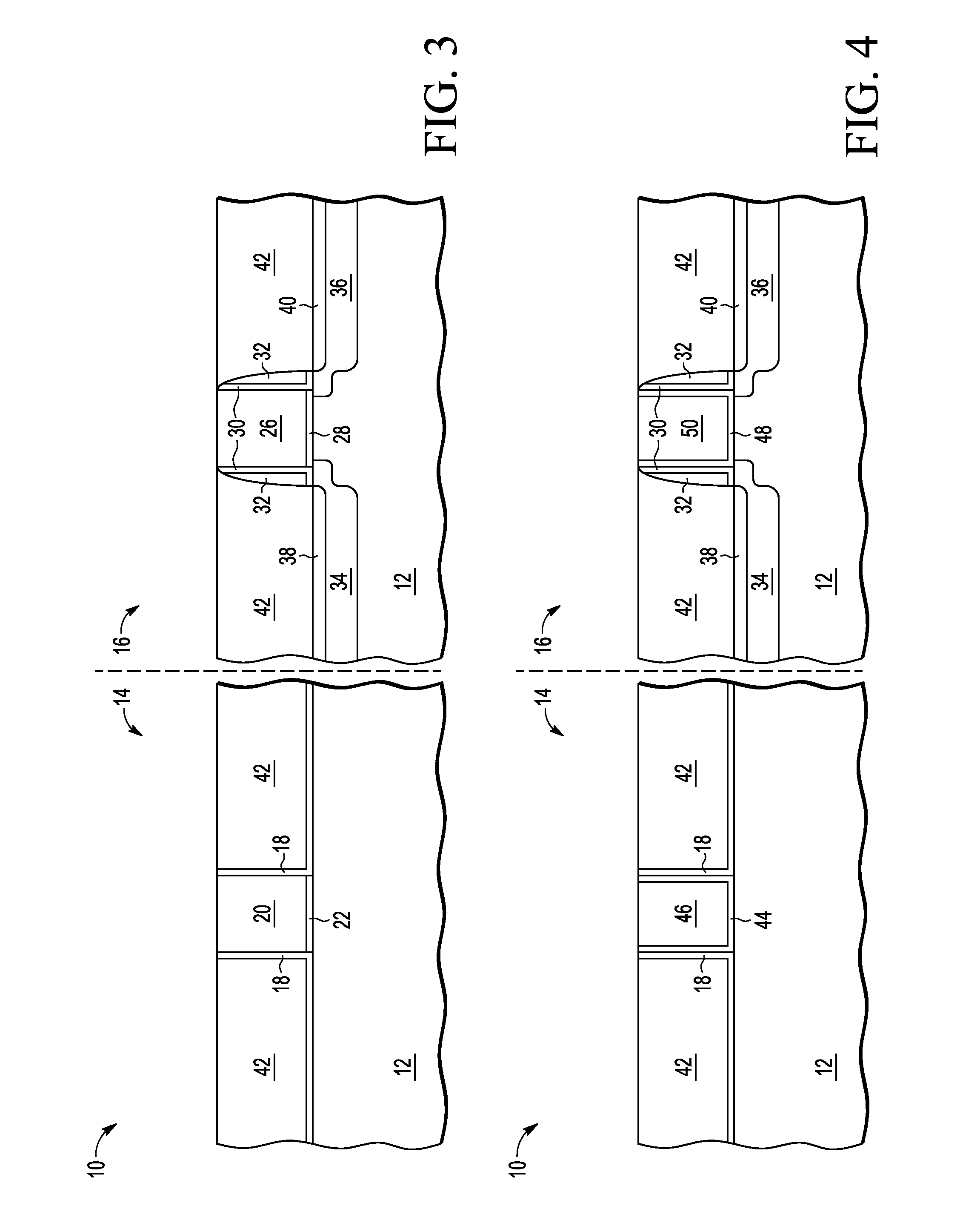
[0017]A non-volatile memory (NVM) cell is made contemporaneously with logic transistors. This can be done with high-k gate dielectrics, metal gates, and metal nanocrystals. In one embodiment, a replacement gate process is used to form both the gate of the logic transistor as well as the metal gate for the select gate of the NVM cell. The source / drain regions for the logic transistors and the silicidation for the logic transistors are formed prior to replacement of the dummy gates in the logic region while the NVM areas remain protected by a protection layer. After replacement of the dummy gates with the actual select gate and actual logic gate, the dielectric layer surrounding the actual select gate is removed from the NVM areas (while being maintained around the logic gate in the logic areas), after which, the charge storage layer and control gate are formed. Furthermore, the source / drain regions and silicidation for the NVM cells can be completed while the logic areas remain prote...


PUM

PropertyMeasurementUnit
thicknessaaaaaaaaaa
chargeaaaaaaaaaa
dielectricaaaaaaaaaa

Abstract

A method of forming an NVM cell and a logic transistor uses a semiconductor substrate. A metal select gate of the NVM cell is formed over a high-k dielectric as is metal logic gate of a logic transistor. The logic transistor is formed, including forming source / drains, while the metal select gate of the NVM cell is formed. The logic transistor is protected while the NVM cell is then formed including forming a charge storage region using metal nanocrystals and a metal control gate over a portion of the metal select gate and a portion of the charge storage region over the substrate. The charge storage region is etched to be aligned to the metal control gate.

Description

BACKGROUND[0001]1. Field[0002]The invention relates to non-volatile memories (NVMs), and more particularly, to NVMs integrated with logic devices.[0003]2. Related Art[0004]Non-volatile memories (NVMs) are often on an integrated circuit which also performs other functions. In such cases it is undesirable to sacrifice logic performance in favor of performance of the NVM. Also it is important to avoid or minimize additional cost in achieving high performance for both the logic and the NVM.[0005]Accordingly there is a need to provide further improvement in achieving high performance while also addressing cost increase issues in integrated circuits that have both NVM and logic.BRIEF DESCRIPTION OF THE DRAWINGS[0006]The present invention is illustrated by way of example and is not limited by the accompanying figures, in which like references indicate similar elements. Elements in the figures are illustrated for simplicity and clarity and have not necessarily been drawn to scale.[0007]FIG....

Claims


Application Information

Patent Timeline
Patent Type & Authority Applications(United States)
IPC IPC(8): H01L21/8239
CPCH01L27/105B82Y10/00H01L21/28273H01L29/42328H01L27/1052H01L29/66825H01L29/7881H01L27/11534H01L29/42332H01L29/66545H01L29/40114H10B99/00H10B41/43
Inventor SHROFF, MEHUL D.HALL, MARK D.
Owner NXP USA INC
Why Eureka
Try Eureka