

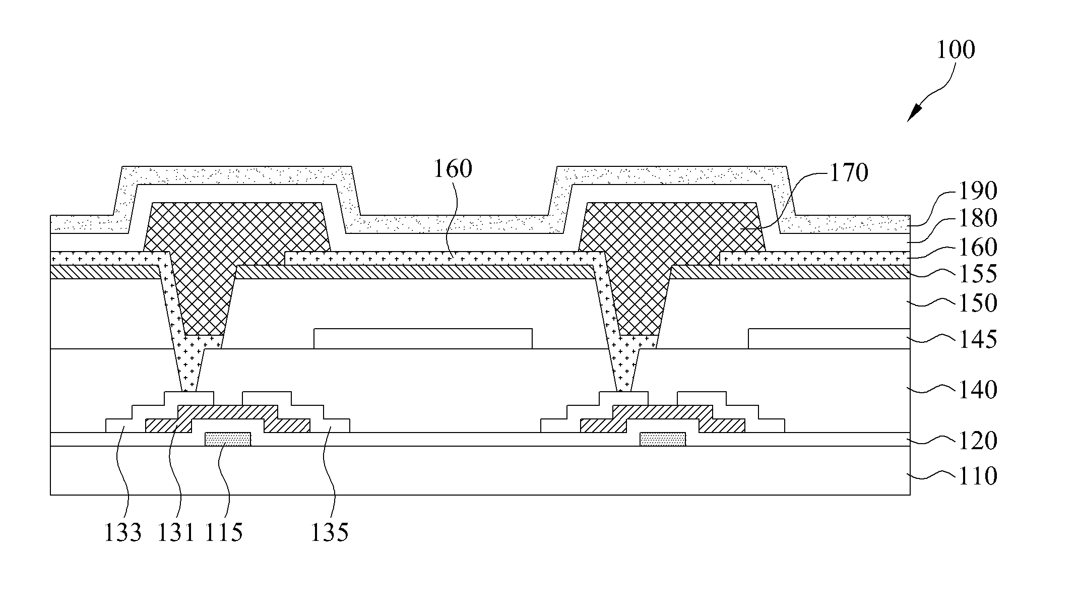
Organic Light Emitting Display Device
a light-emitting display and organic technology, applied in the field of can solve the problems of the above-described organic light-emitting display devices of the related art, and achieve the effect of improving the color reproduction rate, improving the color viewing angle characteristic and the light-emitting efficiency of the panel
- Summary
- Abstract
- Description
- Claims
- Application Information
AI Technical Summary
Benefits of technology
Problems solved by technology
Method used
Image

Examples
experiment example 1
[0108]FIG. 6 is a view showing characteristic which has been analyzed after a doping amount of a yellowish green dopant increases by 14% and 20%, in an organic light emitting display device according to an embodiment of the present invention including a light compensation layer having a thickness of 1600 Å.
[0109]As seen in FIG. 6, the light compensation layer has been formed to have a thickness of 1600 Å, an HTL1 has been formed to have a thickness of 1250 Å, an HL3 has been formed to have a thickness of 350 Å, and an ETL2 has been formed to have a thickness of 450 Å. Also, doping has been performed with the yellowish green dopant in order for the doping amount of the yellowish green dopant to become 14% and 20% compared to the host.
[0110]When the doping amount of the yellowish green dopant is 20% compared to the host, it can be seen that panel efficiency increases, the Voled value decreases, and a color-coordinate change amount decreases, compared to a case in which the doping amou...
experiment example 2
[0116]FIG. 9 is a view showing characteristic which has been analyzed after the doping amount of the yellowish green dopant increases by 14% and 20%, in an organic light emitting display device according to an embodiment of the present invention including a light compensation layer having a thickness of 2200 Å.
[0117]As seen in FIG. 9, the light compensation layer has been formed to have a thickness of 2200 Å, an HTL1 has been formed to have a thickness of 600 Å, an HL3 has been formed to have a thickness of 450 Å, and an ETL2 has been formed to have a thickness of 450 Å. Also, doping has been performed in order for the doping amount of the yellowish green dopant to become 20% (a) and 14% (b) compared to the host.
[0118]When the doping amount of the yellowish green dopant is 20% (a) compared to the host, it can be seen that panel efficiency increases, the Voled value decreases, and a color-coordinate change amount decreases, compared to a case in which the doping amount of the yellowi...
experiment example 3
[0123]FIG. 12 is a view showing characteristic which has been analyzed after the doping amount of the yellowish green dopant increases by 14% and 20%, in an organic light emitting display device according to an embodiment of the present invention having no light compensation layer.
[0124]As seen in FIG. 12, the light compensation layer is not formed, and doping has been performed in order for the doping amount of the yellowish green dopant to become 14% and 20% compared to the host.
[0125]when the doping amount of the yellowish green dopant is 20% compared to the host, it can be seen that panel efficiency increases slightly, the Voled value decreases, and a color-coordinate change amount decreases, compared to a case in which the doping amount of the yellowish green dopant is 14% compared to the host.
[0126]FIG. 13 is a view showing a color-coordinate change amount with respect to a viewing angle, in the experiment example 3 of FIG. 12.
[0127]As seen in FIG. 13, when the doping amount o...
PUM
 Abstract
Description
Claims
Application Information