Discrete Three-Dimensional Memory Comprising Off-Die Read/Write-Voltage Generator

a three-dimensional memory and voltage generator technology, applied in the field of integrated circuits, can solve the problems of large chip area, difficult design of peripheral-circuit components, and inability to meet the requirements of the power supply, so as to reduce the overall cost, minimize the manipulation of power supply, and improve performance

Inactive Publication Date: 2013-07-25
CHENGDU HAICUN IP TECH
View PDF6 Cites 5 Cited by
  • Summary
  • Abstract
  • Description
  • Claims
  • Application Information

AI Technical Summary

Benefits of technology

[0019]It is a principle object of the present invention to provide a three-dimensional memory (3D-M) with a lower overall cost.
[0020]It is a further object of the present invention to provide a 3D-M with an improved performance.
[0021]In accordance with these and other objects of the present invention, a discrete 3D-M is disclosed. The design philosophy behind the discrete 3D-M is to minimize manipulation on power supply, data and address inside a 3D-M die.
[0022]The present invention discloses a discrete three-dimensional memory (3D-M). It comprises at least a 3D-array die and at least a peripheral-circuit die. The 3D-array die comprises a plurality of 3D-M arrays, each of which is formed in a 3-D space and comprises a plurality of vertically stacked memory levels. The peripheral-circuit die is formed on a 2-D plane and comprises a single functional level. It comprises at least one of the peripheral-circuit components. The peripheral-circuit components of the 3D-M include read / write-voltage generator (VR / VW-generator) and address / data translator (A / D-translator).
[0023]Different from the integrated 3D-M where all peripheral-circuit components are located on the 3D-M die, at least one peripheral-circuit component of the discrete 3D-M is located on the peripheral-circuit die. Because the 3D-array die comprises fewer peripheral-circuit component(s), its array efficiency could be larger than 40%. By moving all peripheral-circuit components to the peripheral-circuit die, the array efficiency of the 3D-array die could reach ˜60%.
[0024]Because it is manufactured using an independent process with less complex back-end, the wafer cost of the peripheral-circuit die is much less than the 3D-array die. As a result, the discrete 3D-M is less expensive than the integrated 3D-M for a given storage capacity. In addition, by using discrete 3D-M, the size of the peripheral-circuit components can be reduced. Being a separate die, the peripheral-circuit die can comprise more substrate metal layers (e.g. four vs. two) and therefore, the peripheral-circuit components on the peripheral-circuit die are easier to design and occupy less chip area. Furthermore, because the peripheral-circuit die does not require high-temperature processing, its interconnects may use high-speed interconnect materials, e.g. copper (Cu). This can improve the 3D-M performance.

Problems solved by technology

However, this belief is no longer true for 3D-M.
Because the 3D-M arrays use a complex back-end process while their peripheral circuits use a relatively simple back-end process, integrating the 3D-M arrays with their peripheral-circuit components will force the peripheral-circuit components to use the expensive manufacturing process for the 3D-M arrays.
To make things worse, because they can only use the same number of the substrate metal layers (as few as two) as the 3D-M arrays, the peripheral-circuit components are difficult to design and occupy a large chip area.
This degrades the 3D-M performance.

Method used


Image

  • Discrete Three-Dimensional Memory Comprising Off-Die Read/Write-Voltage Generator
  • Discrete Three-Dimensional Memory Comprising Off-Die Read/Write-Voltage Generator
  • Discrete Three-Dimensional Memory Comprising Off-Die Read/Write-Voltage Generator

Examples


Embodiment Construction

[0039]Those of ordinary skills in the art will realize that the following description of the present invention is illustrative only and is not intended to be in any way limiting. Other embodiments of the invention will readily suggest themselves to such skilled persons from an examination of the within disclosure.

[0040]In the present invention, the symbol “I” means a relationship of “and” or “or”. For example, the read / write-voltage generator (VR / VW-generator) could generate either only the read voltage, or only the write voltage, or both the read voltage and the write voltage; the address / data translator (A / D-translator) could translate either only address, or only data, or both address and data.

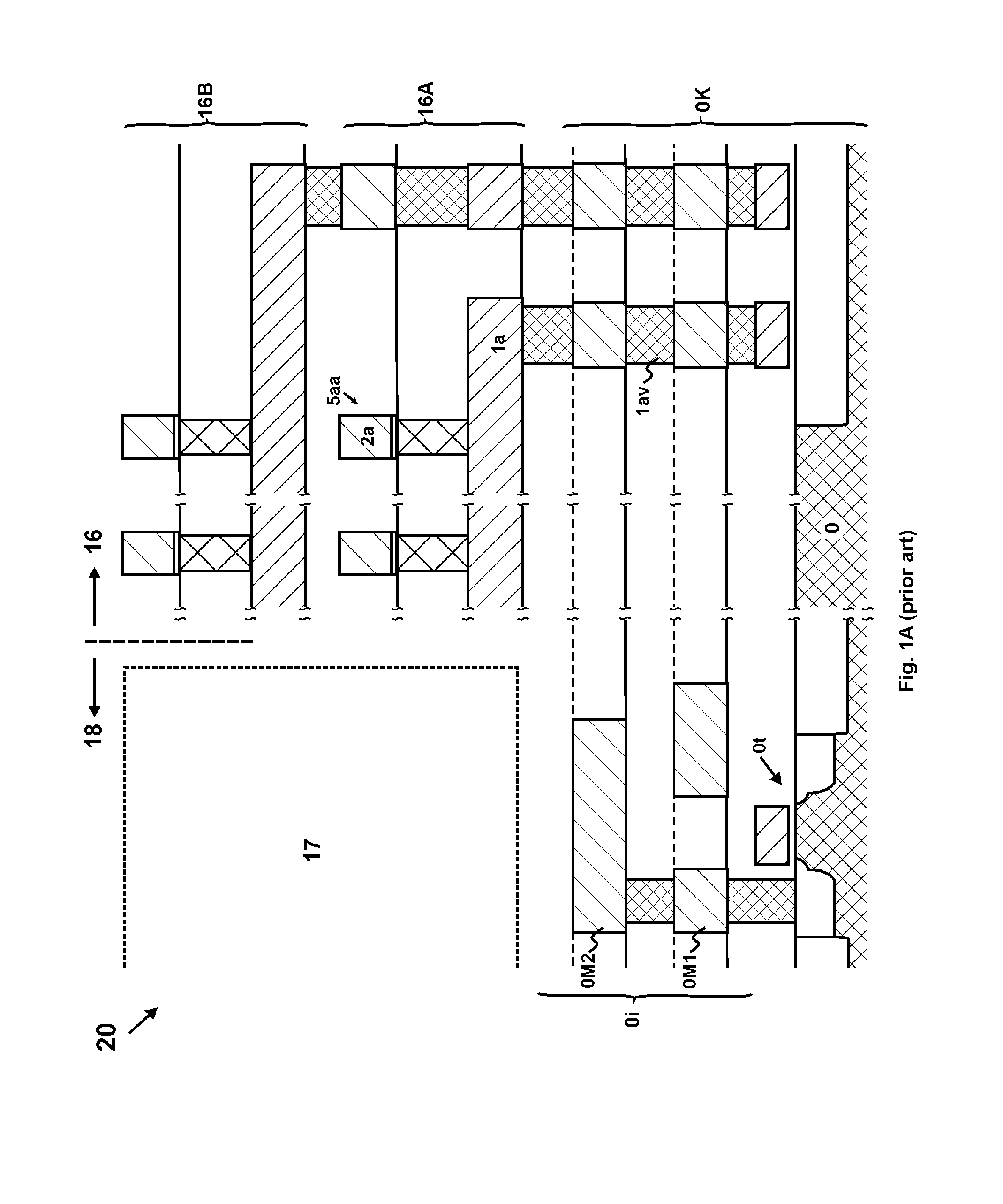
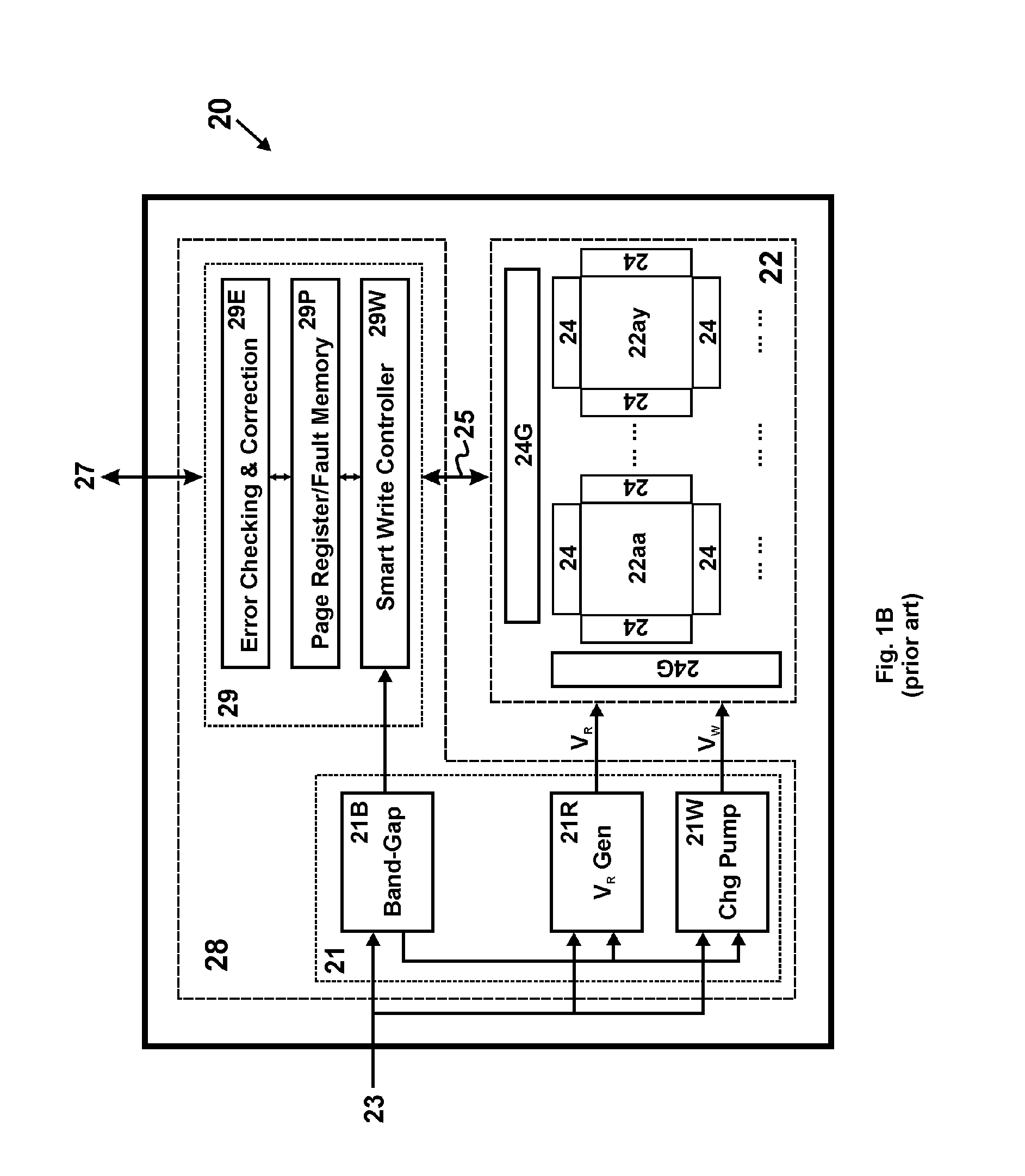
[0041]Referring now to FIGS. 2A-2C, three preferred discrete three-dimensional memory (3D-M) 50 are disclosed. The discrete 3D-M 50 includes a physical interface 54 according to a standard for connecting to a variety of hosts. Physical interface 54 includes individual contacts 52a, 52b, 54a...


PUM


Abstract

The present invention discloses a discrete three-dimensional memory (3D-M). Its 3D-M arrays are located on at least one 3D-array die, while its read/write-voltage generator (VR/VW-generator) is located on a separate peripheral-circuit die. The VR/VW-generator generates at least a read and/or write voltage to the 3D-array die. A single VR/VW-generator die can support multiple 3D-array dies.

Description

CROSS-REFERENCE TO RELATED APPLICATIONS[0001]This is a continuation-in-part of application, “Discrete Three-Dimensional Memory”, application Ser. No. 13 / 591,257, filed Aug. 22, 2012, which relates to a provisional application, “Three-Dimensional Memory with Separate Memory-Array and Peripheral-Circuit Substrates”, Application Ser. No. 61 / 529,929, filed Sep. 1, 2011.BACKGROUND[0002]1. Technical Field of the Invention[0003]The present invention relates to the field of integrated circuit, and more particularly to three-dimensional memory (3D-M).[0004]2. Prior Arts[0005]Three-dimensional memory (3D-M) is a monolithic semiconductor memory comprising a plurality of vertically stacked memory levels. It includes three-dimensional read-only memory (3D-ROM) and three-dimensional random-access memory (3D-RAM). The 3D-ROM can be further categorized into three-dimensional mask-programmed read-only memory (3D-MPROM) and three-dimensional electrically-programmable read-only memory (3D-EPROM). 3D-M...

Claims


Application Information

Patent Timeline
Patent Type & Authority Applications(United States)
IPC IPC(8): G11C13/00
CPCG11C5/145G11C16/30H01L27/11578G11C5/147G11C16/0483G11C16/10H01L27/11551G11C13/0021G11C13/004G11C13/0069G11C5/02H01L25/0657H01L25/105H01L2224/32145H01L2224/32225H01L2224/48145H01L2224/48227H01L2224/73265H01L2225/0651H01L2225/1023H01L2225/1064H01L2225/06506H01L2225/06562G11C8/14H01L2924/00012H01L24/73H10B41/20H10B43/20
Inventor ZHANG, GUOBIAO
Owner CHENGDU HAICUN IP TECH
Why Eureka
Try Eureka