Eddy Current Flaw Detection System and Eddy Current Flaw Detection Method

a flaw detection and eddy current technology, applied in the field of eddy current flaw detection system and eddy current flaw detection method, can solve the problems of inaccurate display distortion, and complicated three-dimensional shape, and achieve the effect of improving the accuracy of evaluation of flaws and the enhancement of display results of flaw detection results

Active Publication Date: 2013-08-01
HITACHI-GE NUCLEAR ENERGY LTD
View PDF57 Cites 19 Cited by
  • Summary
  • Abstract
  • Description
  • Claims
  • Application Information

AI Technical Summary

Benefits of technology

[0010]An object of the present invention is to provide an eddy current flaw detection system and an eddy current flaw detection method capable of enhancing the accuracy of display of a result of flaw detection and improving the accuracy of evaluation of a flaw.
[0012]The present invention is suitable for, for example, a case where a portion on the one side of an eddy current flaw detection probe and a portion on the other side thereof as viewed in the direction intersecting the direction of scanning of the probe are different in terms of the length of a scan trajectory as in the case where the probe is scanned over a surface (inspection surface) of a weld between a reactor pressure vessel and a stub tube of a control rod drive. In order to cope with such a case, in the present invention, three-dimensional coordinates of a plurality of detection points corresponding to combinations (channels) of exciting and detecting coils are acquired for each scan position of the eddy current flaw detection probe. Then, three-dimensional flaw detection data including the three-dimensional coordinates of the detection points and results of detection thereof corresponding to those are created or generated. Further, a three-dimensional model of the inspection surface is displayed, and the results of detection of the detection points are represented in color tones on the three-dimensional model of the inspection surface, based on the three-dimensional flaw detection data. Thus, as compared with the case where as described in JP-2008-8806-A, for example, the scan area is represented by the two-dimensional coordinate system in which each probe scan position and each channel position on the substrate are taken as the coordinates, and detection results of respective channels are represented in color tones of pixels of their corresponding coordinates, no distortion occurs and the accuracy of display of a flaw detection result can be enhanced. As a result, the accuracy of evaluation of the position and length and the like of a flaw can be improved.
[0022]According to the present invention, the accuracy of display of a result of flaw detection can be enhanced, and the accuracy of evaluation of a flaw can be improved.

Problems solved by technology

For example, however, the surface (inspection surface) of the above-described weld between the reactor pressure vessel and the stub tube of the control rod drive is approximately in the form of a truncated conical side surface in its entirety and takes on such a complicate three-dimensional shape that its axial section is concave and its curvature changes depending on a circumferential position.
Thus, when the scan area is represented by the above-described two-dimensional coordinate system, distortion occurs and a result of flaw detection cannot accurately be displayed.
As a result, it is not possible to evaluate the position and length of a flaw accurately.

Method used


Image

  • Eddy Current Flaw Detection System and Eddy Current Flaw Detection Method
  • Eddy Current Flaw Detection System and Eddy Current Flaw Detection Method
  • Eddy Current Flaw Detection System and Eddy Current Flaw Detection Method

Examples


Embodiment Construction

[0043]A first embodiment of the present invention will be described with reference to the accompanying drawings. The present embodiment will be described by taking for example a case where a weld between a reactor pressure vessel and a stub tube of a control rod drive is inspected.

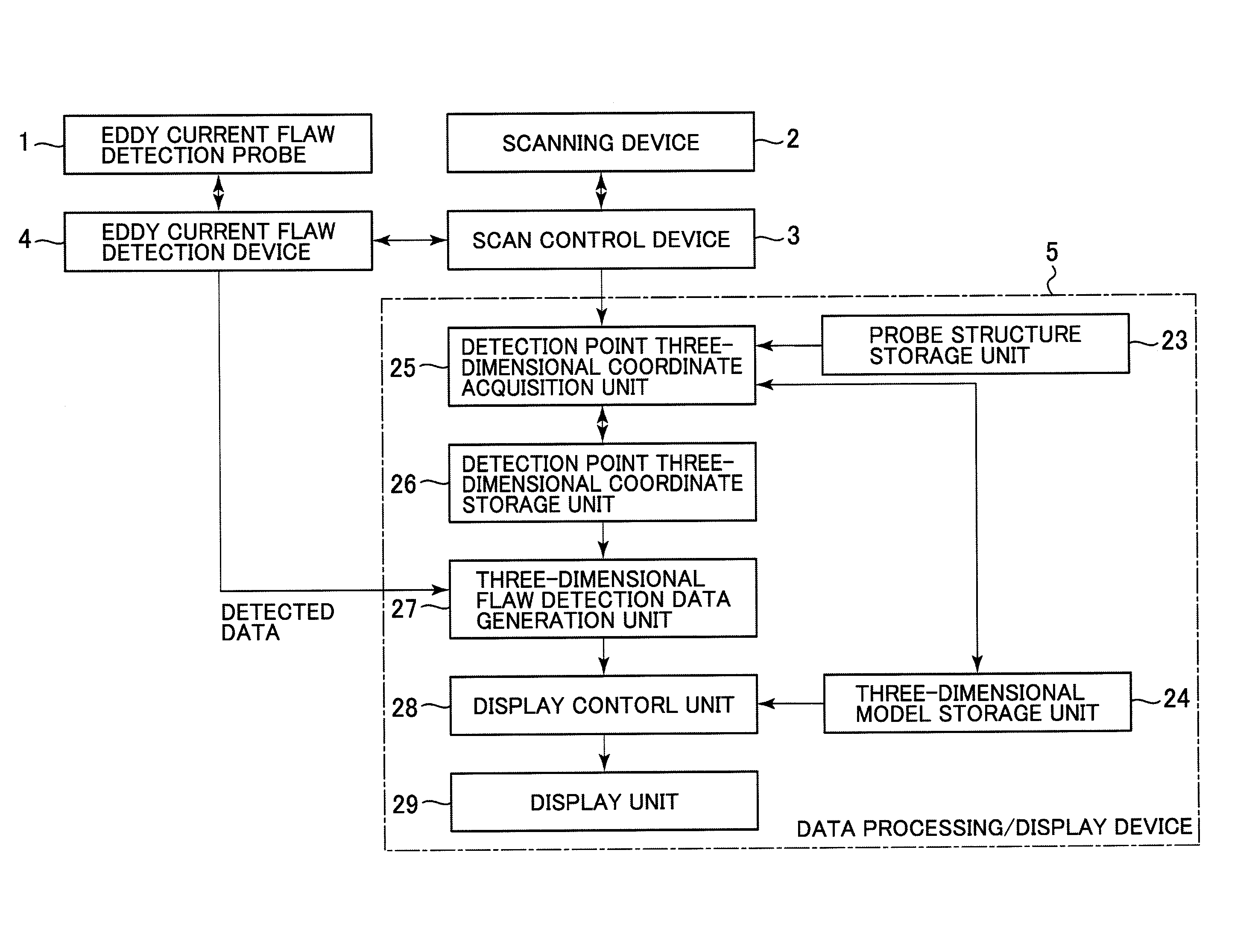
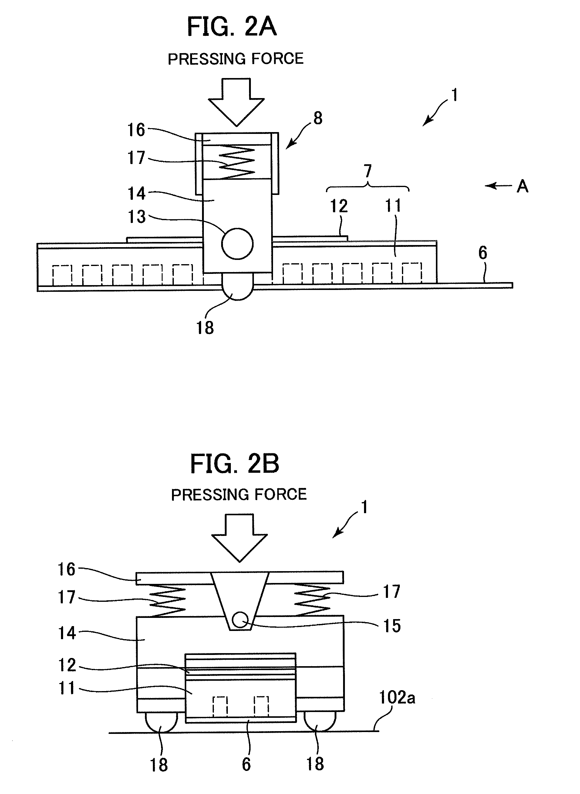
[0044]FIG. 1 is a block diagram showing a configuration of an eddy current flaw detection system according to the present embodiment. FIG. 2A is a side view illustrating an overall structure of an eddy current flaw detection probe in the present embodiment. FIG. 2B is a side view as viewed from a direction indicated by arrow A in FIG. 2A. FIG. 3 is a plan view showing a structure of a sensor part of the eddy current flaw detection probe in the present embodiment. FIGS. 4A and 4B are side views showing a structure of a scanning device in the present embodiment. FIG. 5 is a perspective view for describing the scanning of the eddy current flaw detection probe in the present embodiment.

[0045]The eddy current f...


PUM

PropertyMeasurementUnit
current flaw detectionaaaaaaaaaa
attitude angleaaaaaaaaaa
attitude angle computingaaaaaaaaaa

Abstract

An eddy current flaw detection system includes an eddy current flaw detection probe having a substrate facing an inspection surface, and at least one exciting coil and at least two detecting coils provided on the substrate, a scanning device which scans the probe on the inspection surface, a scan control device which drives and controls the scanning device, an eddy current flaw detection device which acquires results of detection of a plurality of detection points corresponding to combinations of the exciting and detecting coils for each scan position of the probe, and a data processing / display device which processes data from the scan control device and the eddy current flaw detection device and thereby displays a result of flaw detection. The data processing / display device acquires three-dimensional coordinates of the detection points for each scan position of the probe and thereby creates three-dimensional flaw detection data.

Description

BACKGROUND OF THE INVENTION[0001]1. Field of the Invention[0002]The present invention relates to an eddy current flaw detection system and an eddy current flaw detection method for scanning an eddy current flaw detection probe on an inspection surface.[0003]2. Description of the Related Art[0004]An eddy current flaw detection method is an inspection method of causing an alternating magnetic field generated by an exciting coil to induce eddy currents in a surface layer portion of a conductive object to be inspected and detecting a disturbance in eddy currents due to a flaw or crack as a change (change in output voltage) in impedance of a detecting or sensing coil, thereby determining the presence or absence of the flaw.[0005]There has recently been proposed an eddy current flaw detection system using an eddy current flaw detection probe (hereinafter called a “multi-coil probe”) having a plurality of coils arranged on a substrate for the purpose of speeding up inspections (refer to, f...

Claims


Application Information

Patent Timeline
Patent Type & Authority Applications(United States)
IPC IPC(8): G01N27/90
CPCG01N27/9006G01N27/82G01N27/902
Inventor NISHIMIZU, AKIRAKITAZAWA, SOKONO, NAOYUKIENDO, HISASHIOTANI, KENICHIYAMADA, TAIICHIROOUCHI, HIROFUMIYOSHIDA, ISAONONAKA, YOSHIOIMAI, MASAFUMI
Owner HITACHI-GE NUCLEAR ENERGY LTD
Why Eureka
Try Eureka