

Thin film transistor array substrate and method for manufacturing the same
- Summary
- Abstract
- Description
- Claims
- Application Information
AI Technical Summary
Benefits of technology
Problems solved by technology
Method used
Image

Examples
Embodiment Construction
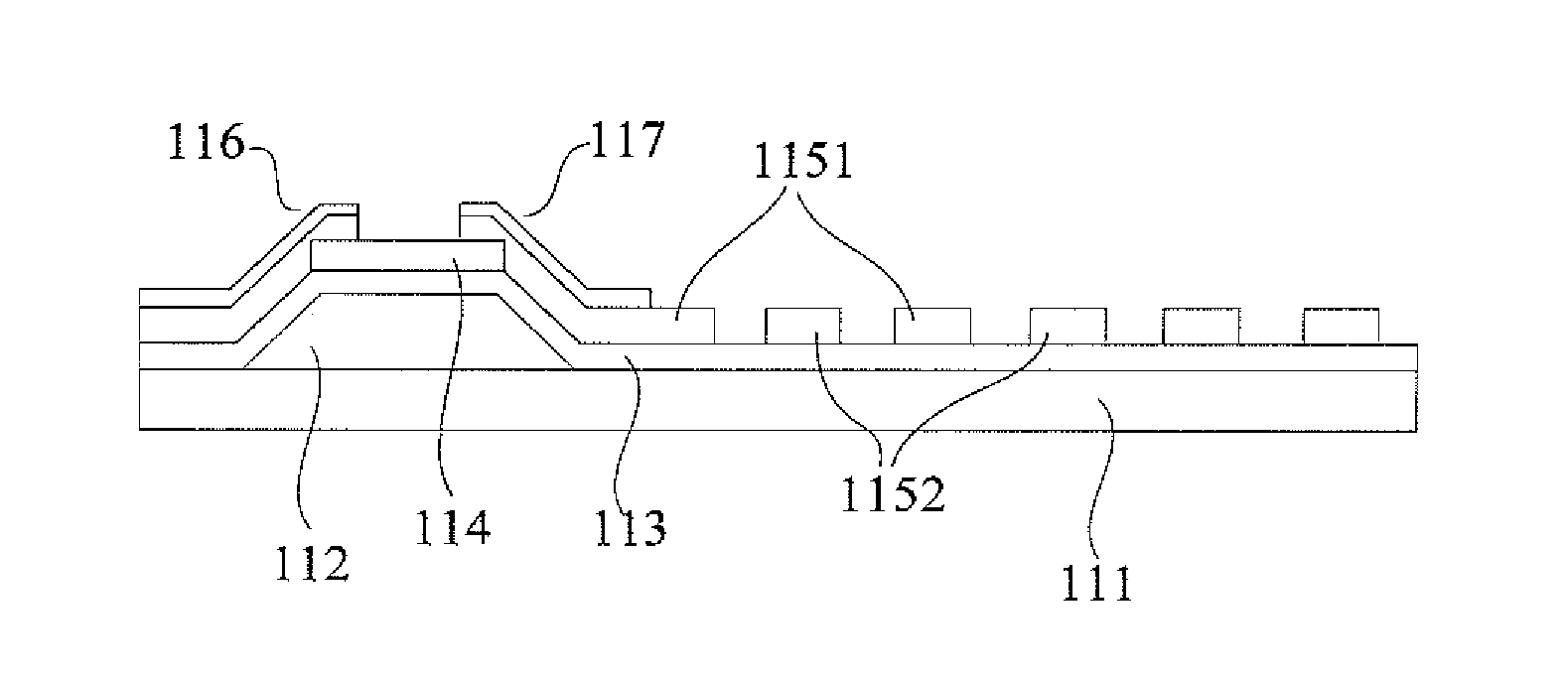
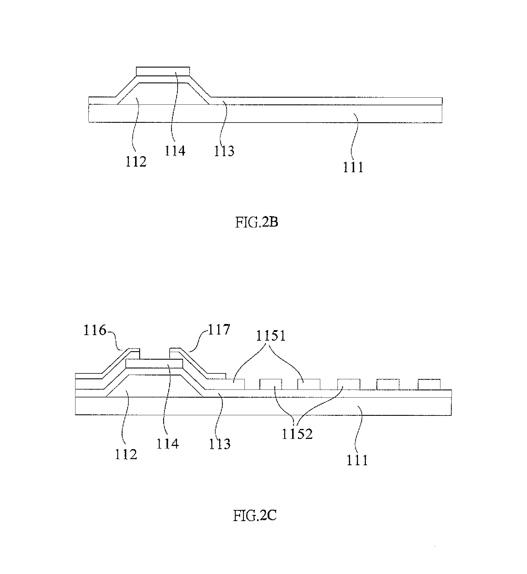
[0031]The following embodiments are referring to the accompanying drawings for exemplifying specific performable embodiments of the present invention. Furthermore, directional terms described by the present invention, such as upper, lower, front, back, left, right, inner, outer, side and etc., are only directions by referring to the accompanying drawings, and thus the used directional terms are used to describe and understand the present invention, but the present invention is not limited thereto.
[0032]In the drawings, structure-like elements are labeled with like reference numerals.
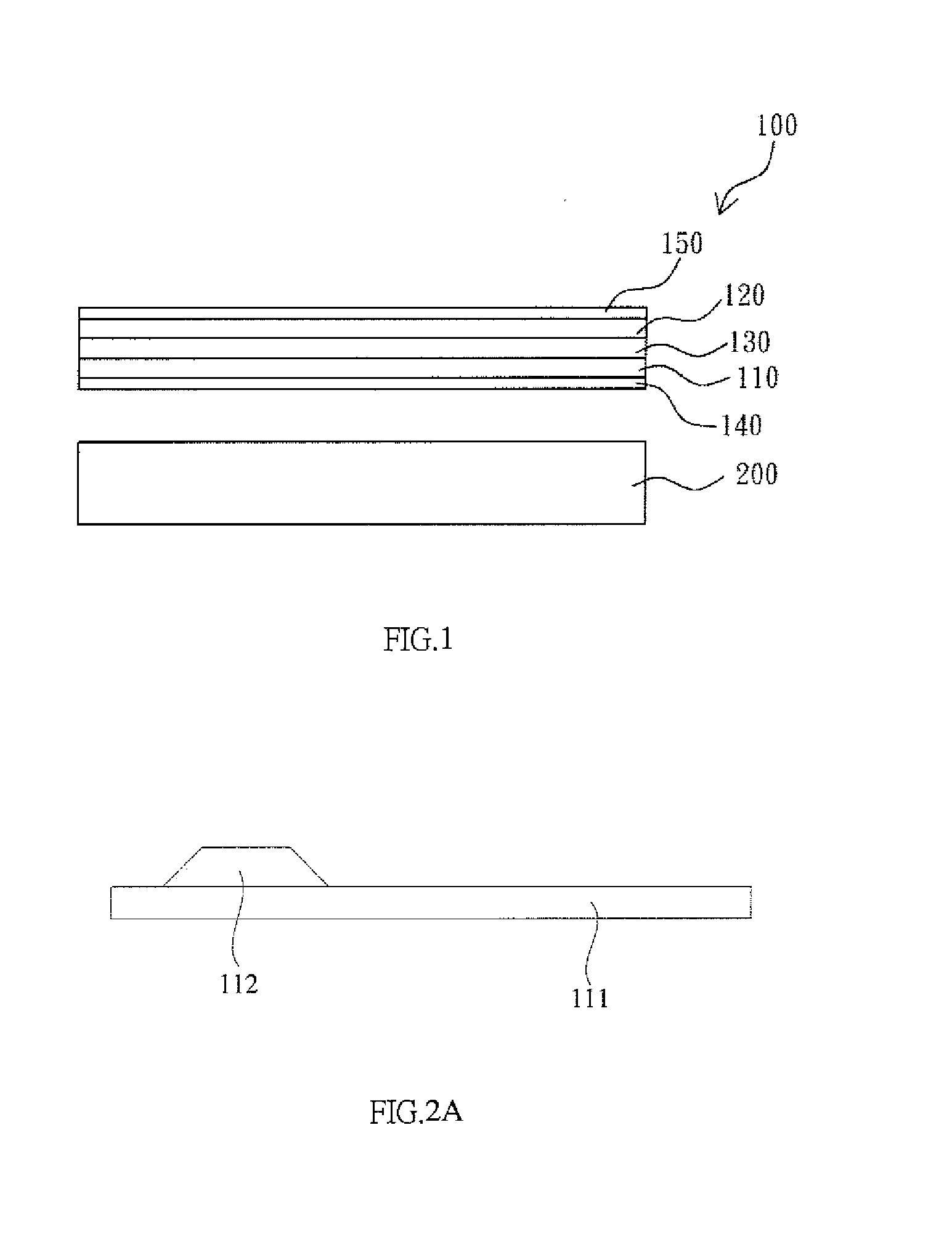
[0033]Referring to FIG. 1, a cross-sectional view showing a display panel and a backlight module according to an embodiment of the present invention is illustrated. The method of the present embodiment for manufacturing a TFT array substrate can be applicable to the fabrication of the display panel 100, such as a liquid crystal display panel. When utilizing the display panel 100 of the present embodiment...
PUM
 Abstract
Description
Claims
Application Information