Method and apparatus for accelerating device degradation and diagnosing the physical changes of the device during the degradation process

a technology of degradation process and device, applied in the field of method and apparatus for testing a device, can solve the problems of inability to diagnose the physical changes within the device, failure may be arbitrarily defined,

Inactive Publication Date: 2013-08-08
UNITED STATES OF AMERICA THE AS REPRESENTED BY THE SEC OF THE ARMY
View PDF2 Cites 12 Cited by
  • Summary
  • Abstract
  • Description
  • Claims
  • Application Information

AI Technical Summary

Benefits of technology

[0005]Embodiments of the present invention comprise methods and apparatus for testing devices. In some embodiments, a method for testing a device includes operating the device in a stress inducing mode using a first set of conditions for a first period of time; determining a first value for a plurality of device parameters after the first period of time; operating the device in the stress inducing mode using the first set of conditions for a second period of time; determining a second value for the plurality of device parameters after the second period of time; and determining if one or more components of the device has at least one of failed or physically changed by comparing the first and second values for the plurality of device parameters.

Problems solved by technology

Failure may be arbitrarily defined, such as when the device operates at lower efficiency or the like.
Unfortunately, testing a device as discussed above may be able to determine the mean time to failure of the device, but may not be able to diagnose the physical changes within the device as it degrades.

Method used


Image

  • Method and apparatus for accelerating device degradation and diagnosing the physical changes of the device during the degradation process
  • Method and apparatus for accelerating device degradation and diagnosing the physical changes of the device during the degradation process
  • Method and apparatus for accelerating device degradation and diagnosing the physical changes of the device during the degradation process

Examples


Embodiment Construction

[0015]Embodiments of the present invention comprise a method and apparatus for testing a device. The inventive methods and apparatus advantageously allow for the determination of one or more failure points or changes of a physical nature in a device under test (DUT). For example, such a determination may identify a specific element or elements of the device that fail or change in some physical manner.

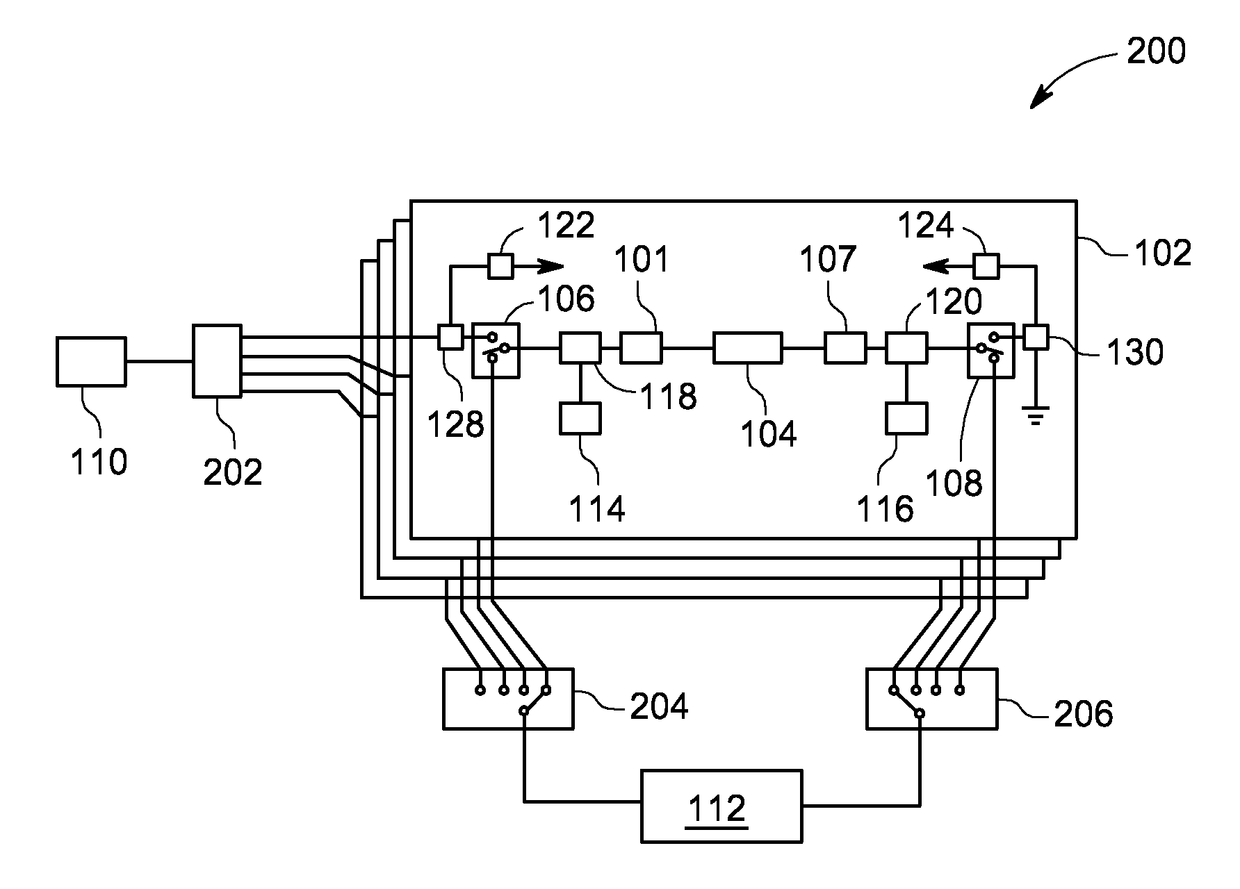
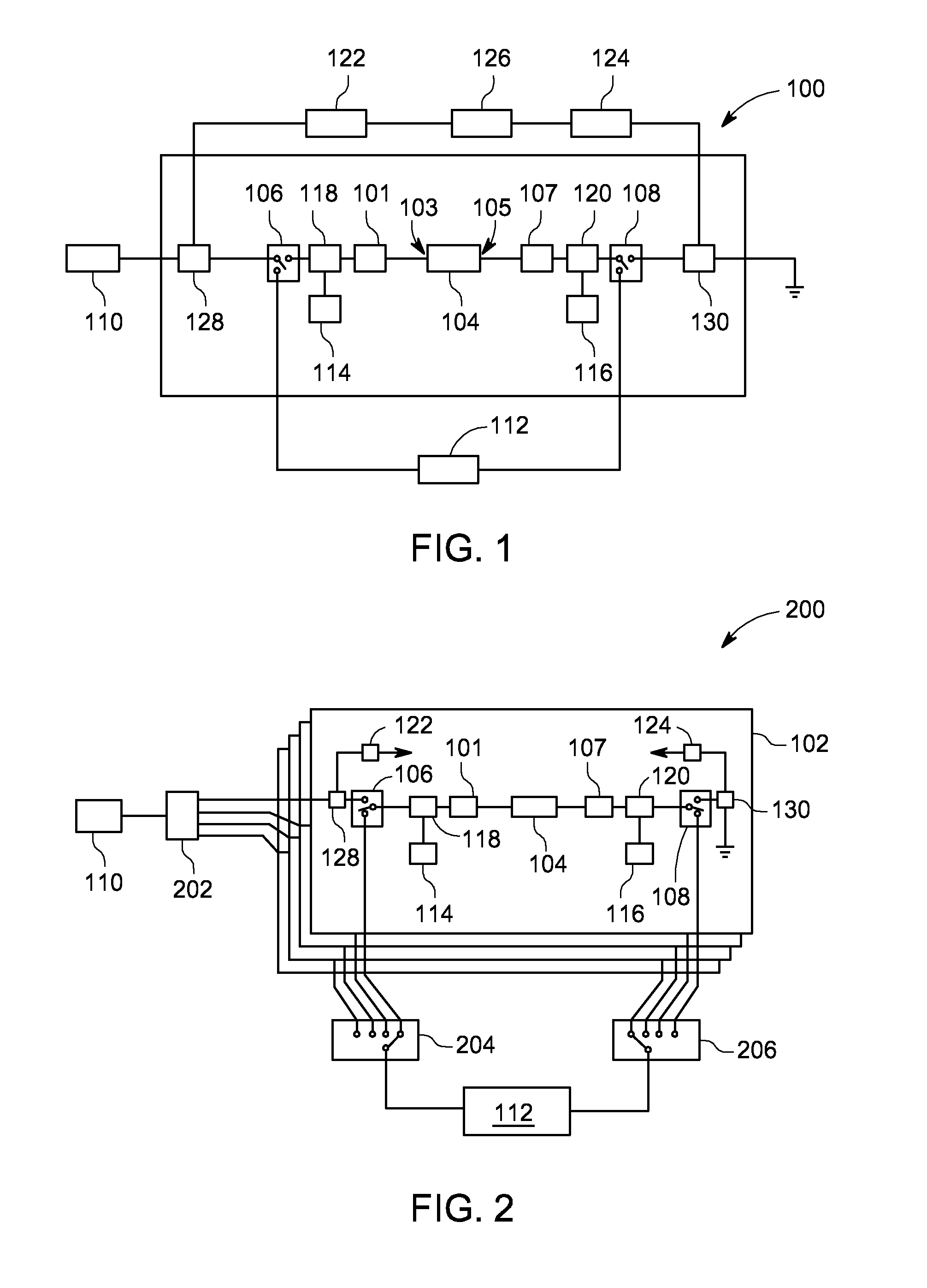
[0016]FIG. 1 depicts an apparatus 100 for testing a device in accordance with some embodiments of the present invention. The apparatus 100 may include a testing platform 102 for testing a device 104 when present on the testing platform 102. The testing platform 102 may include a first switch 106 and a second switch 108, wherein the first and second switches 106, 108 switch the testing platform 102 between a first mode and a second mode. Exemplary first and second switches 106, 108 may include Agilent 8767M RF switches, available from Agilent Technologies of Santa Clara, Calif. However, ...


PUM


Abstract

Embodiments of the present invention comprise methods and apparatus for testing devices. In some embodiments, a method for testing a device includes operating the device in a stress inducing mode using a first set of conditions for a first period of time; determining a first value for a plurality of device parameters after the first period of time; operating the device in the stress inducing mode using the first set of conditions for a second period of time; determining a second value for the plurality of device parameters after the second period of time; and determining if one or more components of the device has at least one of failed or physically changed by comparing the first and second values for the plurality of device parameters.

Description

GOVERNMENT INTEREST[0001]Governmental Interest—The invention described herein may be manufactured, used and licensed by or for the U.S. Government.FIELD OF INVENTION[0002]Embodiments of the present invention generally relate to device testing and, more particularly, to methods and apparatus for testing a device, such as a transistor, amplifier or the like.BACKGROUND OF THE INVENTION[0003]The testing of a device, such as one including a transistor, amplifier, circuit or the like may be performed by operating the device under a stressed condition, such as an elevated temperature, typical operating conditions, or the like, and monitoring the device until it reaches some defined criteria of failure. Failure may be arbitrarily defined, such as when the device operates at lower efficiency or the like. Unfortunately, testing a device as discussed above may be able to determine the mean time to failure of the device, but may not be able to diagnose the physical changes within the device as ...

Claims


Application Information

Patent Timeline
Patent Type & Authority Applications(United States)
IPC IPC(8): G01R31/00
CPCG01R31/2875G01R31/2621
Inventor HUEBSCHMAN, BENJAMIN D.
Owner UNITED STATES OF AMERICA THE AS REPRESENTED BY THE SEC OF THE ARMY
Why Eureka
Try Eureka